Semiconductors, The pnp transistor, The field effect transistor – Elenco Electronic Component Kit User Manual
Page 19
-18-
SEMICONDUCTORS
THE PNP TRANSISTOR
Figure 29 represents the water pipe equivalent of a
PNP transistor. The emitter releases current that
splits into two paths. The base current “forces open”
the collector check valve which collects all the
current except the small amount that goes into the
base. The direction of current in the PNP transistor
is opposite that of the NPN transistor. Because of
these differences, the emitter of the PNP is usually
referenced to the power supply voltage and the
emitter of the NPN is usually referenced to ground
or zero voltage. In both transistors, the current
amplification factor (I
c
/I
b
) is called Beta (
β).
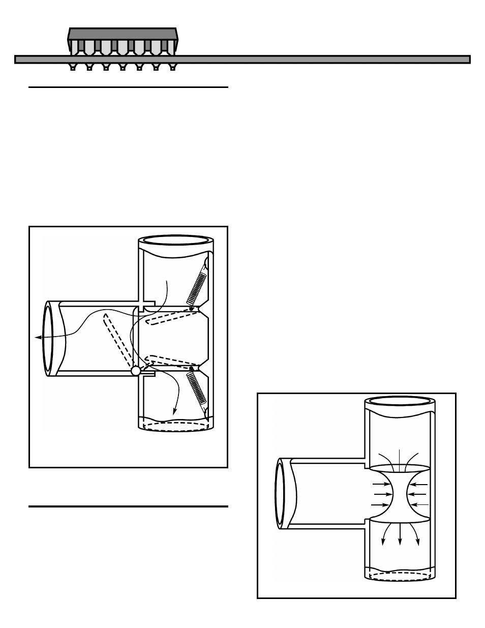
In Figure 30 the center of a small section of a pipe
is made of thin, flexible rubber and that rubber is
surrounded by water from a third pipe called the
gate. When pressure is applied to the gate, the
rubber pinches off the current from the source to the
drain. No current flows from gate to drain or source.
This device uses a change in gate pressure to
control the current flowing from source to drain.
Since there are no check valves, the current can
flow in either direction. In other words, this device
acts like a variable resistor. The Field Effect
Transistor (FET) also controls current between
source and drain by “pinching off” the path between
them. The level of voltage on the gate controls the
amount of current that will flow. Since no DC current
flows in or out of the gate (only momentarily a small
amount will flow to adjust to new pressures as in a
capacitor), the power used by the gate is very close
to zero. Remember, power equals voltage times
current, and if the current is zero, the power is zero.
This is why FET’s are used in the probes of test
equipment. They will not disturb the circuit being
tested by removing power during a measurement.
When a second gate section is added (pipe and
rubber) between the source and drain it is called a
Dual Gate FET. In our water pipe analogy of the
FET transistor, the rubber must be very thin and
flexible in order to “pinch off” the current from the
source to the drain. This means it could be easily
damaged by a small “spike” of high pressure. The
same is true of an electronic FET. A high voltage
“spike” (Static Electricity) can destroy the gate and
ruin the FET. To protect the FET, they are
sometimes packaged with metal rings shorting their
leads, and a fourth lead may be added to the metal
case containing the transistor.
Figure 29
Base
I
B
I
E
= I
B
+ I
C
PNP Transistor
THE FIELD EFFECT TRANSISTOR
Figure 30
Collector
Emitter
I
E
I
C
Drain
Source
Gate
FET Transistor