Semiconductors, What is it, The diode – Elenco Electronic Component Kit User Manual
Page 18: The transistor, Figure 26 figure 27, Figure 28, Npn transistor
-17-
SEMICONDUCTORS
THE DIODE,
what is it?
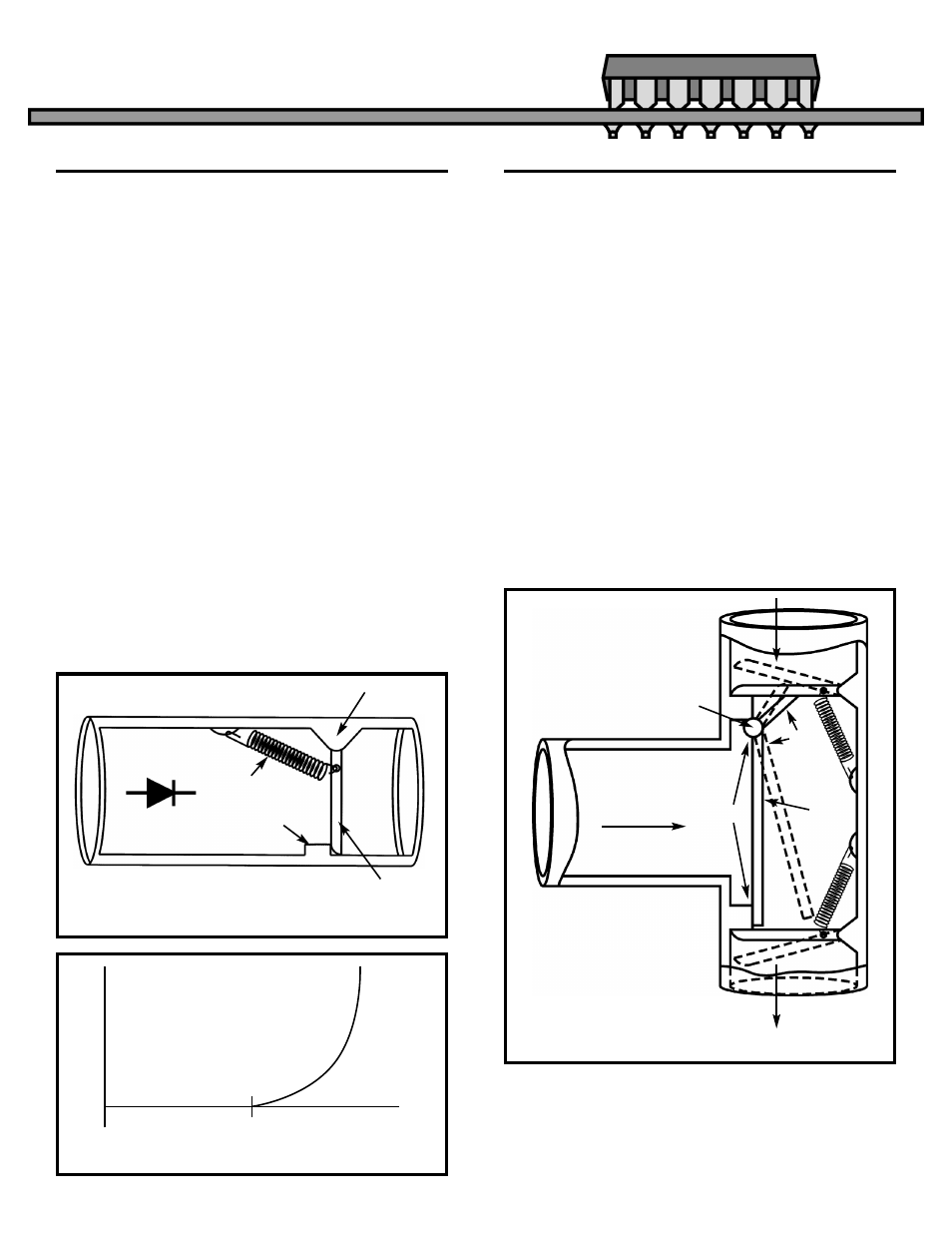
The diode can be compared to the check valve
shown in Figure 26. The basic function of a check
valve is to allow water to flow in only one direction.
Once the force of the spring is exceeded, the plate
moves away from the stop allowing water to pass
through the pipe. A flow of water in the opposite
direction is blocked by the solid stop and plate. If it
took a pressure of 0.7lb to exceed the spring force,
the flow of water versus pressure might look like
Figure 27. In electronics, this curve would represent
the typical silicon diode if pounds per square inch
equaled volts and gallons per minute equaled
amperes. Of course, the amount of current that
flows through the diode must be limited or the device
could be damaged. Just as too much water through
the check valve could destroy the plate (shorted
diode). If the diode is made of Gallium Arsenide, it
would take approximately twice the voltage to
produce a flow of current (spring in Figure 26 is
twice as strong). The energy level required to “turn
on” a Gallium Arsenide diode is so high, that light is
generated when current starts to flow. These diodes
are called “Light Emitting Diodes”, or simply LED’s.
The transistor is best described as a device that
uses a small amount of current to control a large
amount of current (Current Amplifier). Consider a
device fabricated as shown in Figure 28. A small
amount of “Base Current” pushes on the L
1
portion
of the lever arm forcing check valve D
1
to open, even
though it is “reverse biased” (pressure is in direction
to keep check valve shut). Keep in mind the base
current would not start to flow until the check valve
D
2
allowed current to flow (0.7lb). If the current ratio
through D
1
and Base was equal to the lever arm
advantage, then I
1
/ I
b
= L
1
/ L
2
. Call this ratio Beta
(
β) and let L
1
= 1 inch and L
2
= 0.01 inch. Then
β =
100 and I
1
will be 100 times I
b
. Since both currents
must pass through D
2
, I
2
= I
1
+ I
b
. These same
principles apply to a silicon NPN transistor. I
1
becomes collector current (I
C
), and I
2
would be
emitter current (I
E
).
β = I
C
/ I
B
and I
E
= I
B
+ I
C
.
THE TRANSISTOR,
what is it?
Spring
Solid Stop
Movable Plate
Water-tight Pivot
Figure 26
Figure 27
0.7
Pressure (lbs per square inch)
Current (gals
. per min.)
Figure 28
Base Current
I
b
L
1
L
2
I
1
D1
D2
I
2
Lever
Arm
NPN Transistor
Pivot