Video (ttl/vga) interface, Table 3-12, Video interface pin/signal descriptions (j11) – ADLINK CoreModule 430 User Manual
Page 32

Chapter 3
Hardware
26
Reference Manual
CoreModule 430
Video (TTL/VGA) Interface
The Volari Z9s graphics controller provides two graphics display ports for video signals to flat panel
displays and traditional glass CRT monitors. The features are listed below:
•
Enhanced 2D Graphics Controller
Full BitBLT Implementation for all 256 Raster Operations Defined for Windows
Supports 4 Transparent BLT Modes
•
Bitmap Transparency
•
Pattern Transparency
•
Source Transparency
•
Destination Transparency
Rectangle Clipping
Fast Line Draw Engine with styled pattern
Fast Rectangle Fill Engine
256MB frame buffer with linear addressing
64x64x2 bit-mapped mono hardware cursor
•
VGA Output (DB15)
Supports 135 MHz triple RAMDACs for 1280 x 1024 x 75 Hz display
Supports 24-bit pixel depth
Supports interlaced or non-interlaced output
•
TTL Output
Conforms with VESA Flat Panel Display Interface FPDI-1B
Supports up to 1600x1200 pixel display resolutions
Uses Internal CRT Controller for display modes settings
Supports 12-, 18-, and dual 12-bit Interface (1 pixel/clock)
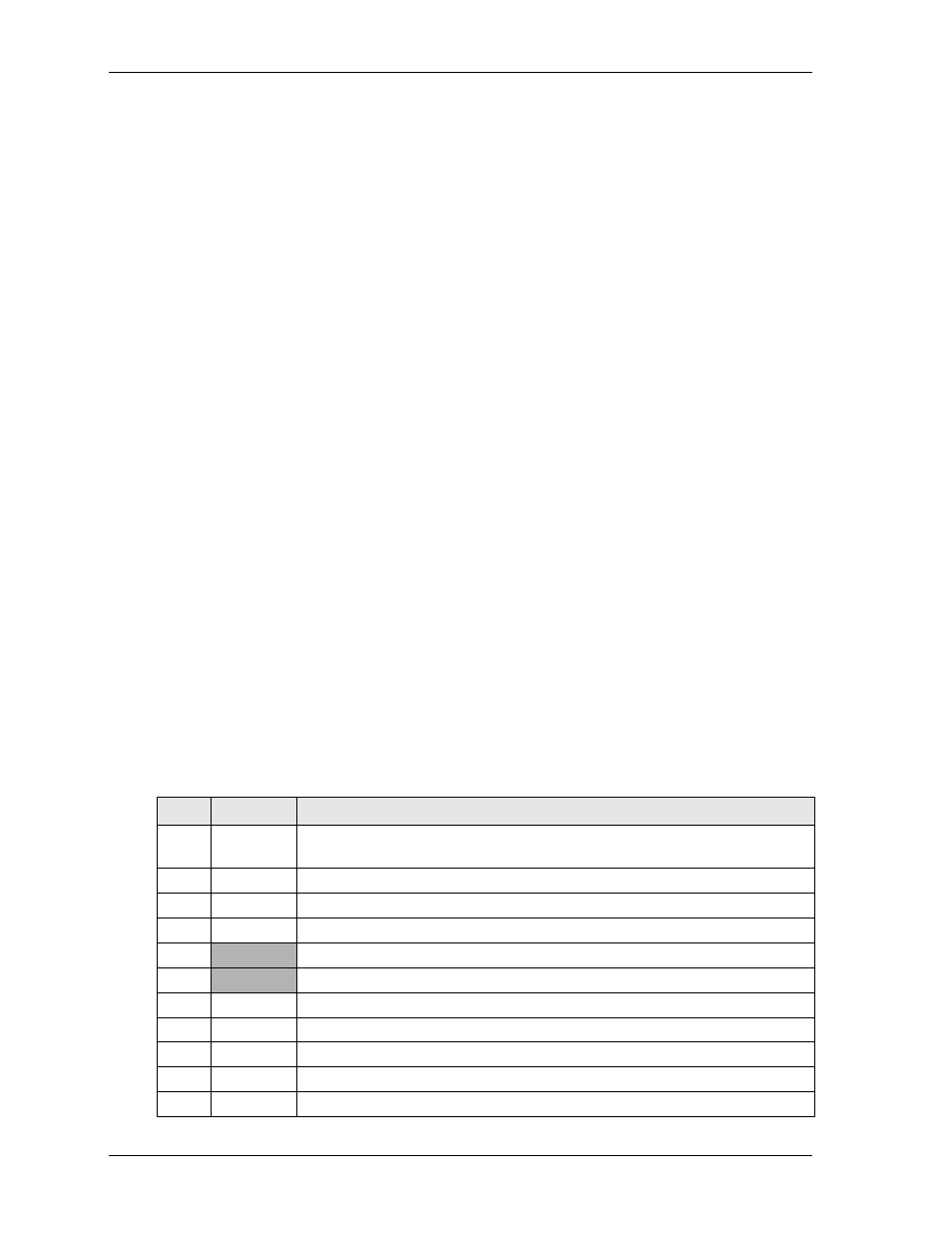
describes the pin signals of the Video interface, which uses a 44-pin, right-angle header with 2
rows, odd/even sequence (1, 2), and 0.079" (2mm) pitch.
Table 3-12. Video Interface Pin/Signal Descriptions (J11)
Pin #
Signal
Description
1
TFTDCLK TFT Shift Clock – This clock signal provides the timing for transferring digital
pixel data.
2
TFTDE
TFT Data Enable – This signal indicates valid data on any of the FP [23:0] lines.
3
TFTLP
TFT Line Pulse – This signal is the digital monitor equivalent of HSYNC.
4
TFTFrame
TFT Frame Marker – This signal is the TFT monitor equivalent of VSYNC.
5
GND
Ground
6
GND
Ground
7
NC
Not connected (FP0 = Panel Data 0)
8
NC
Not connected (FP1 = Panel Data 1)
9
FP2
Panel Data 2 – These pins (0 to 23) provides digital pixel data output signals.
10
FP3
Panel Data 3 – Refer to pin 9, FP2, for more information.
11
FP4
Panel Data 4 – Refer to pin 9, FP2, for more information.
