Minipcie-card-mode jumper header (x20), 12 pc/104 bus interface – ADLINK CM1-86DX2 User Manual
Page 44
38
Module Description
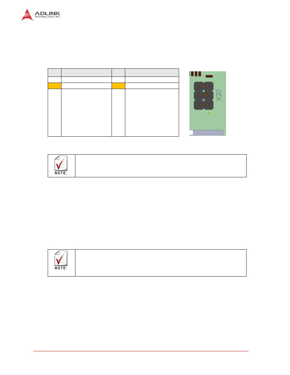
MiniPCIe-Card-Mode Jumper Header (X20)
The default setting is the automatic detection mode (shown below), where pins 3-4 are con-
nected. To force mini card operation, pins 5-6 must be connected. The mSATA mode is forced
by connecting pins 1-2 on the jumper block X20.
3.12 PC/104 Bus Interface
The PC/104 bus is a modification of the industry standard (ISA) PC bus specified in IEEE P996.
The PC/104 bus has different mechanics than P996 to allow for stackable modules. The main
PC/104 features are:
Support for programmable extra wait state for ISA cycles
Support for I/O recovery time for back-to-back I/O cycles
The following table shows the pin assignment of the PC/104 connector.
Table 3-22: PCIe Mini Card Jumper Signals (X20)
Pin
Signal
Pin
Signal
1
+3.3V S
2
SSD-SEL
3
Detection from socket
4
SSD-SEL
5
GND
6
SSD-SEL
Depending on the board used in the Mini PCI Express socket, the automatic switching
between Mini PCI Express and mSATA mode may malfunction. If malfunction occurs,
use Force Mode to switch between mSATA and Mini PCI Express.
-5 V on the PC/104 connector are not supported on this board.
The voltages +5V, +12V, and -12V are not generated by the onboard power-supply but
routed from the Power Supply Connector. The maximum current is limited to 1.0A for
each
voltage.