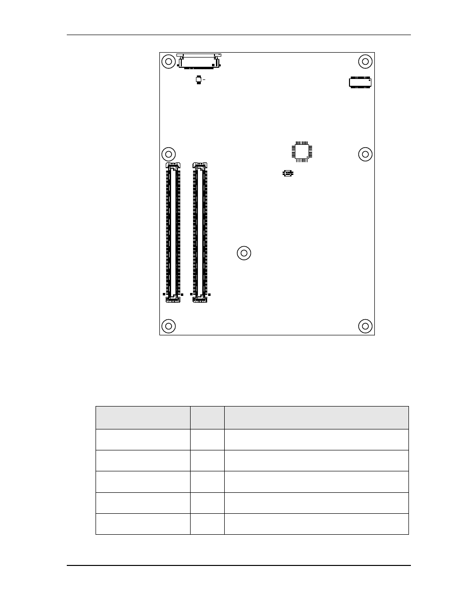
Connectors, headers, and sockets, Figure 2-4, Component locations (bottom side) – ADLINK Express-IBR User Manual
Page 17: Table 2-3, Module connector and socket descriptions, Show the
Chapter 2
Product Overview
Express-IBR
Reference Manual
11
Figure 2-4. Component Locations (Bottom Side)
Connectors, Headers, and Sockets
describes the connectors, headers, and sockets shown in
Table 2-3. Module Connector and Socket Descriptions
Jack/Plug #
Board
Access
Description
J5 – Memory
Top
204-pin socket for un-buffered, ECC DDR3 SODIMM -
Channel A
J6 – Memory
Top
204-pin socket for un-buffered, ECC DDR3 SODIMM -
Channel B
CN1 – XDP Debug (see
.)
Bottom
26-pin, 0.020" (0.50mm) right-angle debug port connector
for the CPU and PCH
CN4 – LPC Debug
Top
10-pin, .050" (1.27mm) female debug port header for
issues such as Port 80 POST errors
CN6 – COM Express A-B
(see
.)
Bottom
220-pin standard connector for Northbridge Video and
Southbridge I/O functions
U8
Express-IBR_Bottom_Comp_a
Key:
U6 - Hardware Monitor
U8 - Board Controller
U42 - I²C EEPROM
U6
U42