3 ssi_trig2 and ssi_start_op, Ssi_trig2 and ssi_start_op – ADLINK PCI-9846 User Manual
Page 59
Operation Theory
49
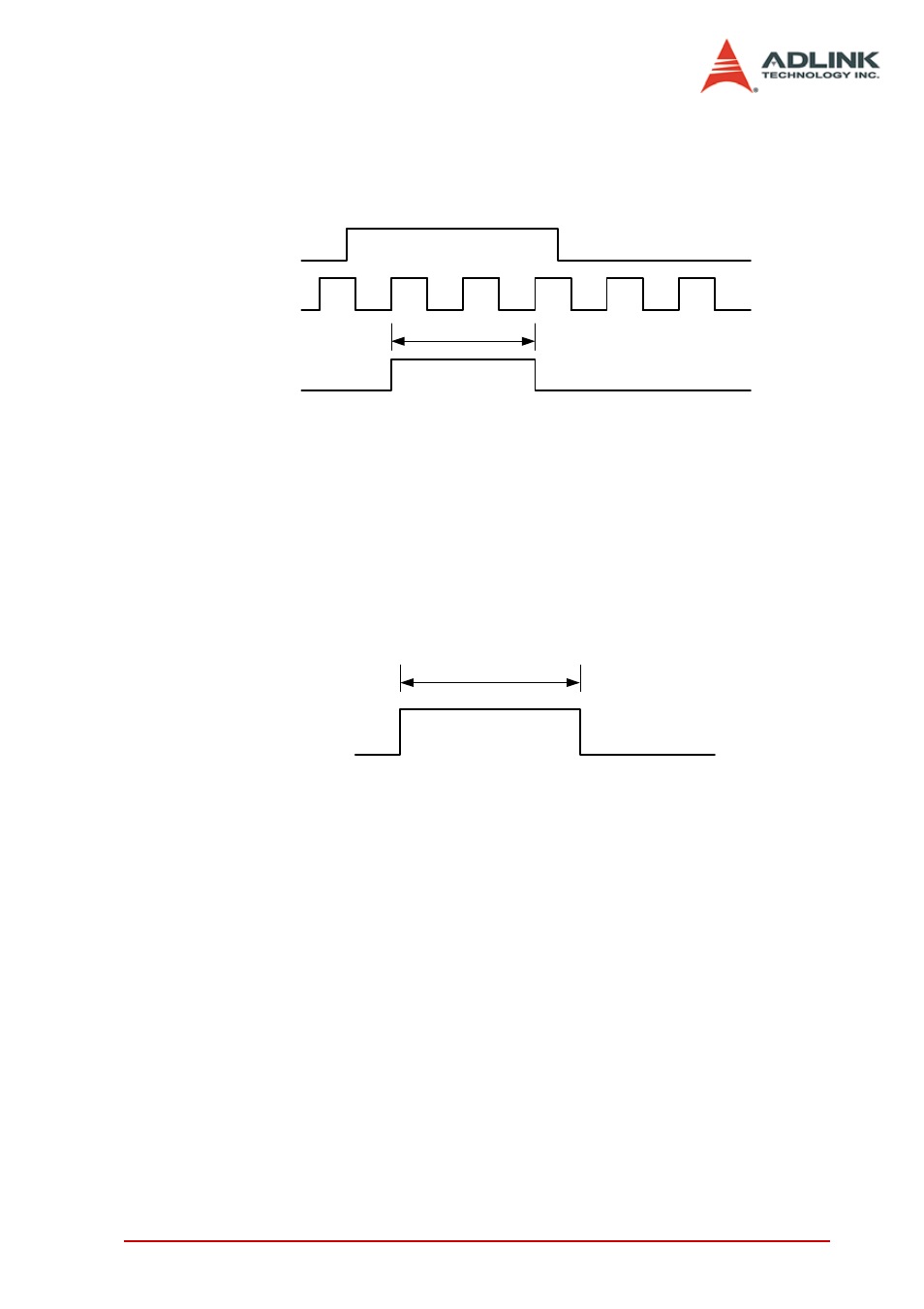
3.7.3 SSI_TRIG2 and SSI_START_OP
As an output, the SSI_TRIG2 signal is a clocked SSI_TRIG1 sig-
nal by TIMEBASE, as illustrated in Figure 3-22.
Figure 3-22: SSI_TRIG2 Output Timing
As an input, the PCI/PXI-9816/26/46 accepts the SSI_TRIG2 sig-
nal to be the source of a one-clock delayed trigger event. The con-
troller on the PCI/PXI-9816/26/46 will then compensate the one-
clock delay if using SSI_TRIG2 as the source of trigger event. The
signal is configured in the rising edge-detection mode.
Figure 3-23: SSI_TRIG2 Input Timing Requirement
As an output, the SSI_START_OP signal reflects the operation
start signal in a pre-trigger or middle-trigger acquisition sequence.
Please refer to Figure 3-12 - Figure 3-14 for the relationship
between the operation start signal and the acquisition sequence.
As an input, the PCI/PXI-9816/26/46 accepts the SSI_START_OP
signal to be the operation start signal in a pre-trigger or middle-
trigger acquisition sequence. The signal is configured in the rising
edge-detection mode. Figure 3-24 show the SSI_START_OP sig-
nal input and output timing requirements.
SSI_TRIG1
Tw
Tw = 2 TIMEBASE Clocks
TIMEBASE
SSI_TRIG2
SSI_TRIG2
Tw
Tw = 20 ns minimum