2 basic ai acquisition, 1 analog input path, 2 basic acquisition timing – ADLINK PCI-9846 User Manual
Page 38: Basic ai acquisition, Analog input path basic acquisition timing, Figure 3-3: analog input signal block diagram, 28 operation theory
28
Operation Theory
3.2 Basic AI Acquisition
In this section, we are going to explain the basic acquisition timing.
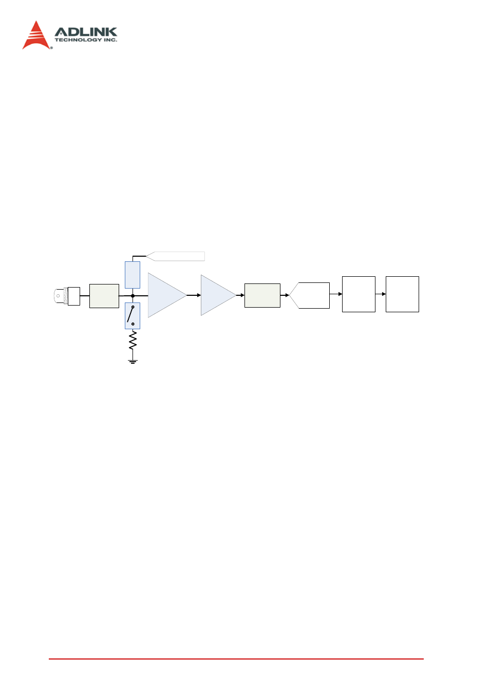
3.2.1 Analog Input Path
The following figure shows the block diagram of the single analog
input path of a digitizer. Each path provides a choice of 50 Ω input
impedance or high impedance. The gain amplifier is optimized for
each input range with low noise and high dynamic range. An anti-
aliasing filter is also adopted to eliminate high frequency noise.
The 16-bit ADC provides not only accurate DC performance but
also high signal-to-noise ratio, high spurious-free dynamic range
in AC performance.
Figure 3-3: Analog Input Signal Block Diagram
3.2.2 Basic Acquisition Timing
The trigger is a signal that starts or stops the acquisition. In post-
trigger mode and delay trigger mode, the trigger is used to initiate
acquisition. In pre-trigger mode, the trigger is used to stop acquisi-
tion. In middle-trigger mode, the trigger is used to inform the acqui-
sition engine to acquire the specific number of data and then stop.
Timebase is a clock that sent to the ADC of each channel and the
acquisition engine for essential timing functionality. The source of
timebase can be either internal oscillator or external clock genera-
tor. Usually the maximum sampling rate of a digitizer is determined
by the speed of timebase. However, other sampling rate can be
achieved by specifying a scan interval counter. Please refer to
Table 3-1 below and Section “3.3.4” on page 32 for more details.
50O
Anti-aliasing
Filter
Calibration Source
Protection
Circuitry
Gain Amplifier
Hi Impedance
Buffer
16-bit
40M/20M/10M
ADC
Onboard
Memory
PCI Interface