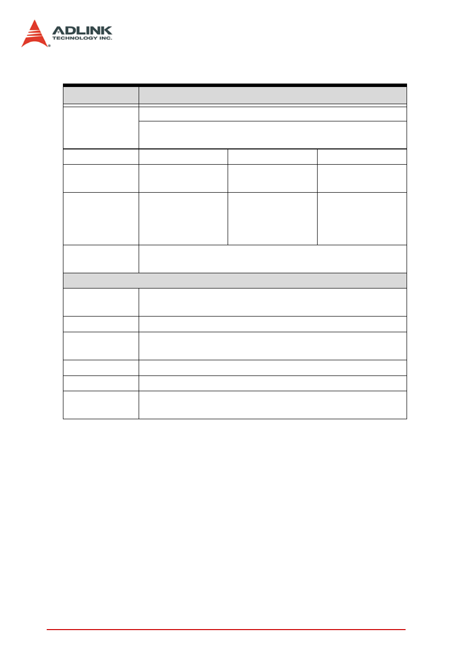
Table 1-8: timebase – ADLINK PCI-9846 User Manual
Page 24
14
Introduction
Timebase
Specification
Value
Sample Clock
Sources
Internal: onboard oscillator
External: CLK IN (front panel SMB connector), PXI STAR,
PXI Trigger Bus[0..7], PXI 10MHz, SSI bus
PCI/PXI-9816
PCI/PXI-9826
PCI/PXI-9846
Timebase Fre-
quency Range
10 MHz-1 MHz
20 MHz-1 MHz
40 MHz-1 MHz
Sampling Rate
Range (24-bit
divided coun-
ter)
10 MS/s-0.596 S/s 20 MS/s-1.192 S/s 40 MS/s-2.384 S/s
Internal Oscil-
lator Stability
±25 ppm
CLK IN (external clock from front panel)
Connector
Type
SMB
Clock Type
Sine wave or square wave
Input Imped-
ance
50 Ω
Input Coupling AC
Input Range
1VP-P to 2VP-P
Overvoltage
Protection
2.5 V
P-P
Table 1-8: Timebase