7 synchronizing multiple modules, Synchronizing multiple modules, Table 3-4: summary of ssi timing signals and – ADLINK PCI-9846 User Manual
Page 54: The corresponding function
44
Operation Theory
3.7 Synchronizing Multiple Modules
The eight interconnected lines on PXI backplane named as PXI
Trigger Bus[0:7] provide a flexible interface for multiple modules
synchronization. The PXI-9816/26/46 utilizes the PXI Trigger
Bus[0:7] as the System Synchronization Interface (SSI). By pro-
viding flexible routing of timebase clock and trigger signals onto
PXI Trigger Bus, the PXI-9816/26/46 makes the synchronization
between multiple modules easy and simple.
For PCI-9816/26/46, a dedicate connector is served as system
synchronization interface. With this interface, PCI-9816/26/46 is
capable of achieving multiple module synchronization. Following
figure shows the installation of multiple module synchronization.
The bi-directional SSI I/Os provide a flexible connection between
modules, which allows one SSI master PCI/PXI-9816/26/46 to out-
put the SSI signals to other slaves modules to receive the signals.
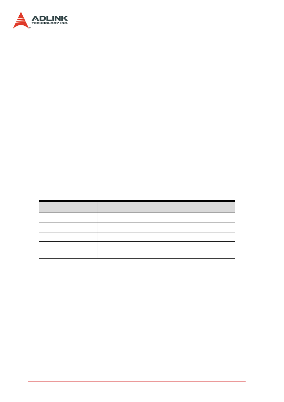
Table 3-4 lists the summary of SSI timing signals and the function-
alities. Figure 3-18 shows the architecture of SSI. Note that it’s not
allowed to route different signals onto the same trigger bus line.
SSI Timing Signals
Functionality
SSI_TIMEBASE
Input/output timebase signal through SSI
SSI_TRIG1
Input/output trigger signal through SSI
SSI_TRIG2
Input/output clocked trigger signal through SSI
SSI_START_OP
Input/output the acquisition start signal in pre-trig-
ger or middle-trigger mode
Table 3-4: Summary of SSI timing Signals and the Corresponding Function