3 adc sampling rate and timebase control, 1 internal oscillator, 2 external clock through front panel – ADLINK PCI-9846 User Manual
Page 41: Adc sampling rate and timebase control, Internal oscillator, External clock through front panel, Pxi_star (pci version), Pxi trigger bus[0 ] (pxi version), Pxi 10m (pxi version), Operation theory 31
Operation Theory
31
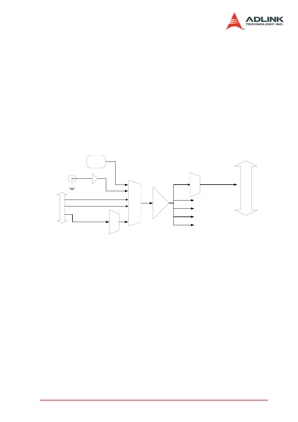
3.3 ADC Sampling Rate and TIMEBASE Control
The PXI/PCI-98X6 supports several timebase sources for analog
input conversion:
Internal oscillator
External clock through front panel
PXI_STAR (PCI version)
PXI Trigger Bus[0..7] (PXI version)
PXI 10M (PXI version)
SSI (PCI version)
The following diagram shows the timebase architecture of the PXI/
PCI-98X6.
Figure 3-5: PCI/PXI-98x6 Timebase Source and Architecture.
3.3.1 Internal Oscillator
The PCI/PXI-9816/26/46 equips a high stability, low jitter oscillator
for the ADCs. The oscillators are 10 MHz, 20 MHz and 40 MHz for
PCI/PXI-9816, PCI/PXI-9826 and PCI/PXI-9846, respectively.
3.3.2 External Clock Through Front Panel
When you need a specific timebase in some applications that the
onboard oscillator is not achievable, a clock from an external
device can replace onboard oscillator. In addition, external time-
base also provides a method to synchronize digitizers to other
measurement modules by distributing/receiving a common clock
to/from multiple modules. The PCI/PXI-9816/26/46 can receive an
8-to-
1 MUX
T
ime
ba
se
C
lock M
u
x
P
X
I In
ter
fa
ce
PXI Trigger Bus[0:7]
PXI_STAR
Ext. CLK IN
SMB
Connector
ADC3
PXI T
ri
g
ge
r Bus
or
SSI
PXI_10M
Onboard
Oscillator
ADC0
ADC1
ADC2
8-to-1 MUX
1-to-5 Cloc
k
Bu
ffe
r
CLK Buffer