9 writing bank-switched code, 1 hardware overview, 2 software overview – Maxim Integrated 71M6534 Energy Meter IC Family Software User Manual
Page 35: Writing bank-switched code, Hardware overview, Software overview

71M653X Software User’s Guide
4.9 WRITING BANK-SWITCHED CODE
The 80515 microcontroller contained in the 71M653X Energy Meter chips can only address 64Kbytes of code. This
section explains how to design firmware with more than 64K of code for the 71M653X Energy Meter chips.
4.9.1 Hardware Overview
In the 71M6531 there is a 32K area from code address 0x0000 to 0x7FFF. The code in this area is always available to
the 8051. This area is “common” and is the same memory area as “bank 0”. Since it is always present, it never needs
to be switched into the bank area.
A 32K bank is selected by writing the bank’s number in the register FL_BANK, an SFR at 0xB6. After this, the bank’s
code is visible to the MPU in addresses 0x8000 to 0xFFFF.
The 71M6531 has four 32K banks (128K bytes total). Bank 0 is the common area. Banks 1, 2, and 3 are the banked
code areas selected by FL_BANK.
The 71M6534 has eight 32K banks (256K total). Bank 0 is the common area. Banks 1 through 7 are the banked code
areas selected by FL_BANK.
A reset sets FL_BANK to 1, so any 71M653x IC can run 64K of non-bank-switching code.
The 71M653x ICs have two write protect registers to protect ranges at the beginning and end of flash.
The beginning is protected by BOOT_SIZE, XDATA 0x20A7 when WRPROT_BT is set in FLSHCTL, SFR 0xB2.
The end can be protected by placing the CE program at the start of the area to protect, and setting WRPROT_CE in
FLSHCTL, SFR 0xB2.
FL_BANK
[2:0]
Address Range for
Lower Bank
(Common)
(0x000-0x7FFF)
Address Range for
Upper Bank
(0x8000-0xFFFF)
6531
128KB
6533
128KB
6534
256KB
000
0x0000-0x7FFF
0x0000-0x7FFF X X X
001
0x0000-0x7FFF
0x8000-0xFFFF X X X
010
0x0000-0x7FFF
0x10000-0x17FFF
X X X
011
0x0000-0x7FFF
0x18000-0x1FFFF
X X X
100 0x0000-0x7FFF 0x20000-0x27000
X
101 0x0000-0x7FFF
0x28000-0x2FFFF
X
110 0x0000-0x7FFF 0x30000-0x37FFF
X
111 0x0000-0x7FFF
0x38000-0x3FFFF
X
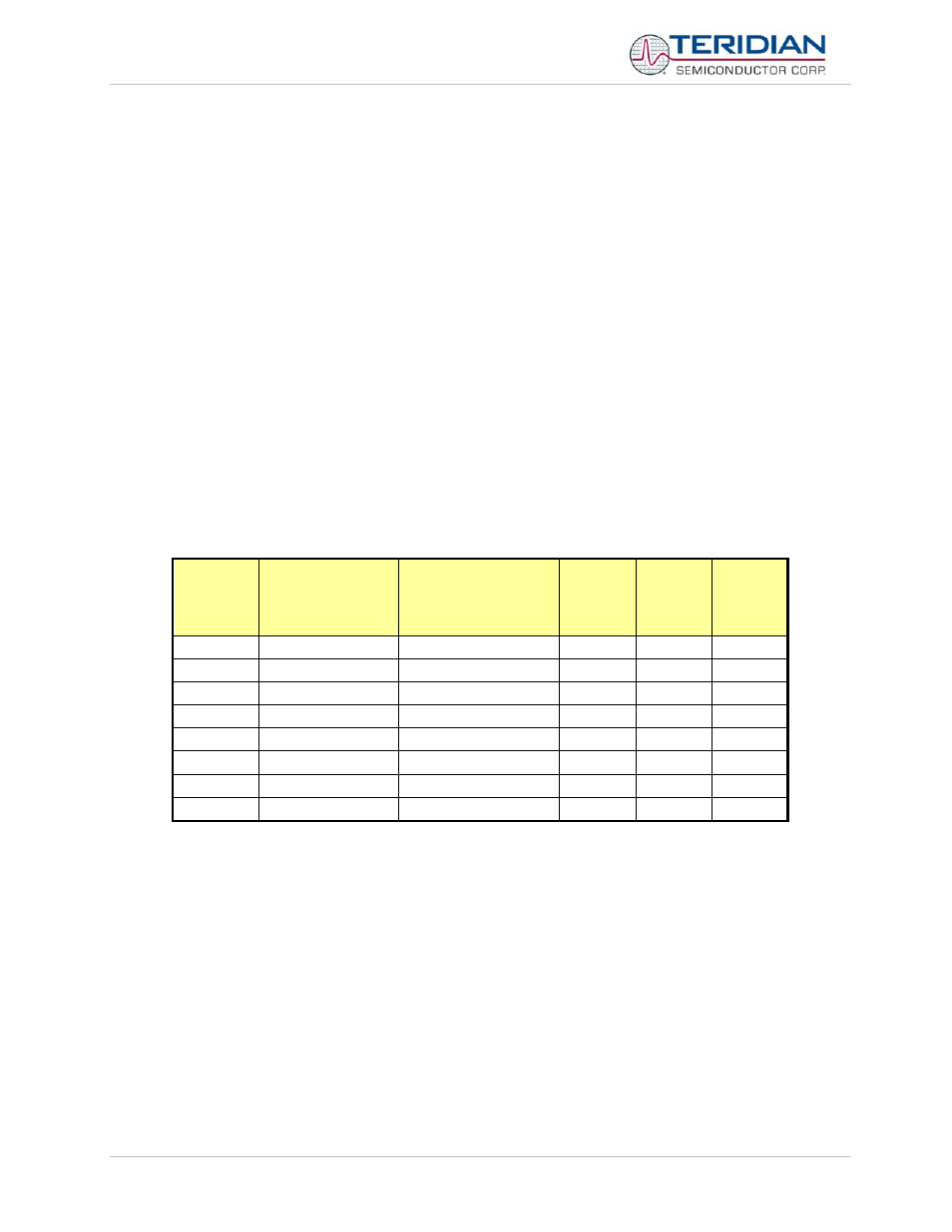
Table 4-1: Code Bank Memory Addresses and Availability
The 71M653x ICs’ flash memory are very similar to the ROM arrangement in Keil’s example “Banking With Common
Area” of chapter 9 (linker) of Keil’s “Macro assembler and Utilities” manual.
4.9.2 Software Overview
Teridian’s demonstration code uses the Keil compiler’s standard bank switching system (www.Keil.com).
This is completely supported by Keil, a major compiler vendor for 8051s, and Signum, the emulator vendor. Code can
be ported from non-banked projects, and full symbolic banked debugging is available.
Keil’s scheme puts a “page table” in common memory. Code calls an entry in the page table. Each entry is a bit of
code that switches to the subroutine’s bank, and jumps to the subroutine in the bank.
Keil’s linker automatically produces the page table. In Teridian’s demo code, the size of this table is less than 1K.
Code using the page table is slower than native 16-bit code, because it has to set the page register.
v1.1v1.1
TERIDIAN Proprietary
35 of 116
© Copyright 2005-2008 TERIDIAN Semiconductor Corporation
