Digilent Pegasus Board User Manual
Page 9
Pegasus Reference Manual
Digilent, Inc. ™
www.digilentinc.com
Page
9
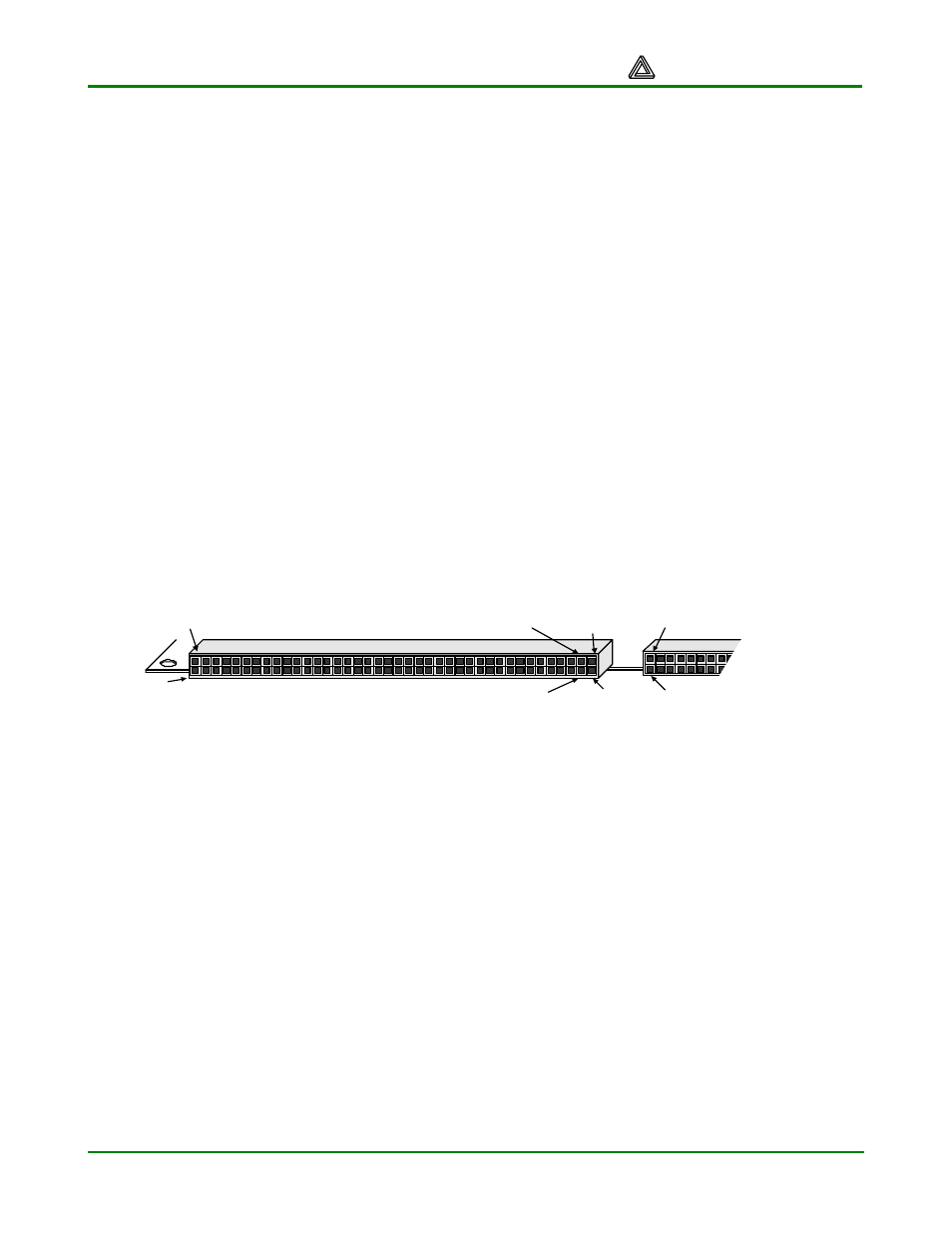
Pin 1: GND
Pin 2: VU
Pin 3: 3.3V
Pin 4
Pin 39
Pin 40
Figure 7. Expansion Connector Pins
decoding logic for sync pulse generation.
Expansion Connectors
40-Pin Connectors
Three expansion connectors labeled A1, A2,
and B1 are available on the Pegasus board.
These female socket connectors mate with
100-mil spaced, 2x20 right-angle headers
(available at most distributors). All three
connectors have GND on pin 1, VU on pin 2,
and 5V on pin 3. Pins 4-35 route to FPGA I/O
signals, and pins 36-40 are reserved for JTAG
and/or clock signals (see Figure 13).
Each of the expansion connectors provides 32
unique I/0 signals. These signals have been
grouped into three different types of busses for
documentation purposes, and to facilitate
communications with external boards. The
lower 18 pins (pins 4-21) of the A1 and B1
connectors are designated as the “system
bus”. The system bus defines eight data
signals, six address lines, two strobes (WE and
OE), a chip select, and a clock. The lower 18
pins of the A2 connector are designated as the
“peripheral bus”, and the individual pins are not
assigned any further definitions. The upper 14
pins of each expansion connector (pins 22-35)
have been designated as “module busses”.
Module bus pin definitions are consistent with
enhanced parallel port (EPP) pin definitions,
and they include eight address/data lines,
three strobes (address write, data write, and
read/write), and three status lines (wait, reset,
and initialize). Figure 13 below shows
expansion connector signal routing. Some
Digilent peripheral boards use the system bus
pins. Bus timings mimic a simple 8-bit
microprocessor bus, with signal timings shown
in figure 14 below. Module boards (like the
USB or Ethernet boards) use the module bus.
Module bus timings are consistent with EPP bus
timings.
6-Pin Connector
The Pegasus board also contains a 6-pin
accessory port (J1). This port provides Vdd,
GND, and four unique FPGA signals. Several 6-
pin module boards that can attach to this
connector are available from Digilent, including
speaker boards, H-bridge boards, sensor
boards, etc.
Peripheral Bus
System Bus
The “system bus” is a protocol used by certain
expansion boards that mimics a simple 8-bit
microprocessor bus. It includes eight data lines,
six address lines, a write-enable (WE) strobe
that can be used by the peripheral to latch
written data, an output-enable (OE) strobe that
can be used by the peripheral to enable read
data, a chip select, and a clock to enable
synchronous transfers. Figure 14 shows bus
signal timings used by Digilent to create bus
controllers in peripheral devices. However, any
bus and timing model can be used by modifying
circuits in the FPGA and attached peripheral
devices.
Module Bus
The module bus protocol is used by various
module boards (like the Ethernet and USB
modules) to communicate with the Pegasus
board. The module bus signals and timings are
borrowed from the EPP protocol. Timings and
signals are shown here.