Digilent Pegasus Board User Manual
Page 2
Pegasus Reference Manual
Digilent, Inc. ™
www.digilentinc.com
Page
2
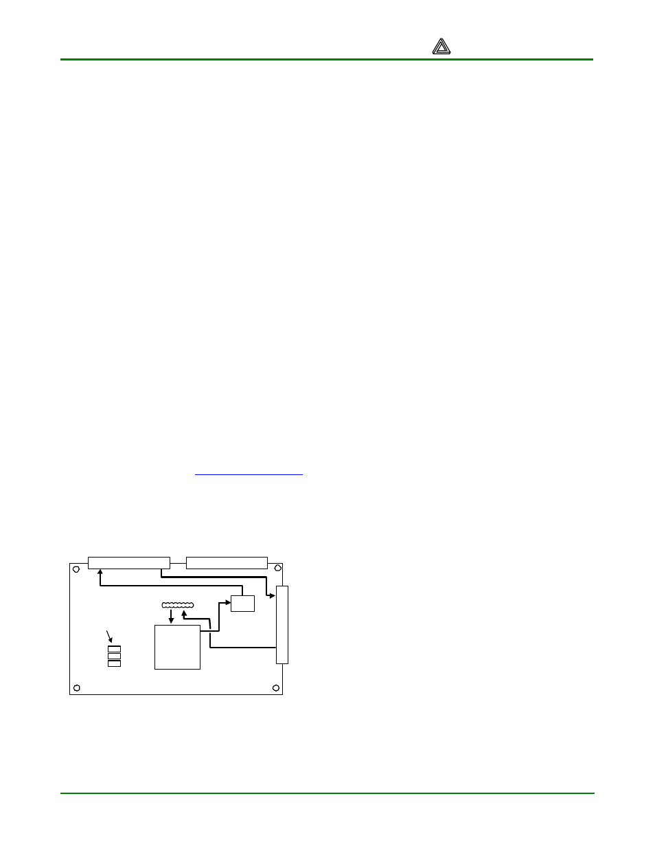
JTAG Ports and Device Configuration
The Spartan 2 FPGA, the XCF01S Platform
Flash ROM, and any programmable devices
on peripheral boards attached to the Pegasus
board can be programmed through JTAG
ports. The JTAG scan chain is routed from the
primary JTAG connector (port 1) to the FPGA,
Platform Flash, and two connection ports as
shown in Figure 2. The primary configuration
port (Port 1) uses a standard 6-pin JTAG
header (J6) that can accommodate Digilent’s
JTAG3 cable (or cables from Xilinx or other
vendors). The other two bi-directional JTAG
ports are available on the A1 and B1
expansion connectors. If no peripheral boards
are present on these connectors, a buffer on
the Pegasus board removes them from the
JTAG chain. If a peripheral board with a JTAG-
programmable device is attached, the scan
chain is driven out the expansion connector so
that the device can be configured. If a Digilent
port module is connected to A1 or B1, then the
port module can drive the JTAG chain to
program all devices in the scan chain. Port
modules include Ethernet, USB, EPP parallel,
and serial modules. (See
www.digilentinc.com
for more information). For port modules to
drive the JTAG chain, a jumper must be
installed on the primary JTAG connector
across the TDI and TDO pins.
A1
A2
B
1
JTAG connector
Programming
mode select
jumpers
Port 2
Platform
Flash
Spartan 2E
PQ 208
P
o
rt
3
(Port 1)
Figure 2. JTAG signal routing on Pegasus
To program the Pegasus board from the
primary port, first power on the Pegasus board,
then connect it to the PC with a JTAG cable,
and then run the “auto-detect” feature of the
configuration software. The configuration
software will identify all devices in the scan
chain, and then each device can be bypassed
or programmed with a suitable configuration
file. Note that both the FPGA and Platform
Flash ROM will always appear in the scan
chain. If the Platform Flash ROM is loaded with
an FPGA configuration file, the FPGA will load
that file at power-on if jumpers are loaded in all
three positions of J4 (M2, M1, and M0).
Power Supplies
The Pegasus board requires a regulated 5V
power supply (it ships with a 5V regulated wall-
plug supply). If a higher voltage supply is used,
the Pegasus board may be permanently
damaged. The power supply is connected to
the Pegasus board using a 5.5mm OD, 2.5mm
ID center-positive power jack. The 5V supply
from the power jack is connected directly to the
V
CCIO
supply that drives the FPGA I/O signals,
and to a 2.5V regulator that supplies the
Spartan 2 V
CORE
voltage.
Total board current is dependant on FPGA
configuration, clock frequency, and external
connections. In test circuits with roughly 20K
gates routed, a 50MHz clock source, and all
LEDs illuminated, approximately 200mA +/-
30% of supply current is drawn from the 2.5V
supply, and approximately 100mA is drawn
from the 5V supply. Required current will
increase if peripheral boards are attached.
The Pegasus board uses a four layer PCB,
with the inner layers dedicated to VCC and
GND planes. Most of the VCC plane is at 5V,
with an island under the FPGA at 2.5V. The
FPGA and the other ICs on the board all have
0.047uF bypass capacitors placed as close as
possible to each VCC pin. The power supply
routing and bypass capacitors result in a very
clean, low-noise power supply.
Oscillators
The Pegasus provides a 50MHz SMD primary
oscillator and a socket for a second oscillator.