Digilent 6003-210-012P User Manual
Page 9
6
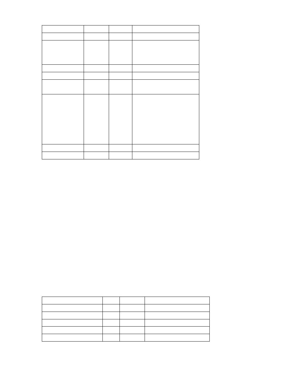
Signal Name
Pin
Voltage
Description
LCD Data 3
G24
2.5V
As above
LCD Data 4
G25
2.5V
Four high order bi-directional
tristate data bus pins. Used for
data transfer and receive
between the MPU and the
ST7066.
LCD Data 5
H25
2.5V
As above
LCD Data 6
H26
2.5V
As above
LCD Data 7
G27
2.5V
As above. Additionally DB7
can be used as a busy flag.
LCD - RS
C19
2.5V
Register Select. 0: Instruction
register (for write) and busy
flag and address counter for
read.
1: Data register for read and
write
LCD – R/W
D20
2.5V
Read (1)/ Write(0) control
LCD – E
C18
2.5V
Enable -
Starts data read/write.
Table 6. LCD FMC Connections
7.
Both the (a and b) stereo head set jack and a mono speaker jack are controlled via potentiometer
volume control (7c). Dual DAC121S101s (12-bit) digital to analog converters (DACs) provide stereo input
into a LM4838 2W Stereo Audio Amplifier. Each 12-bit DAC supports a data rate of up to 30MHz and is
compatible with SPI, QSPI, NICROWIRE, and DSP interfaces. The effective conversion rate is has a
conversion frequency of about 1.75MHz – well above the audio range. Both DAC outputs (right and left
channels) are then fed in the Audio Amplifier and are available through a mono speaker connector (left
channel only) on J5, and a stereo headphone connector on J6. Both output volumes are controlled via
the potentiometer R47, which is clearly labeled on the board.
Key specifications for part DAC121S101 from National Semiconductor:
DNL: +0.25, -0.15 LSB (typ)
Output Settling Time: 8 us (typ)
Zero Code Error: 4mV
Full Scale Error: -0.06%
Signal Name
Pin
Voltage
Description
Audio DAC clock left
H37
2.5V
30MHz max SPI
Audio DAC data left
G37
2.5V
16 bit frames
Audio DAC sync left
H38
2.5V
Marks start of data frame
Audio DAC clock right
H35
2.5V
30MHz max SPI
Audio DAC data right
H34
2.5V
16 bit frames