Notes, Au\ Page 99
Page 99
Attention! The text in this document has been recognized automatically. To view the original document, you can use the "Original mode".
2180 A
DIGITAL <-5v/
NOTES:
1. UNiLESS OTHERWISE SPECIFIED ALL RESISTANCES AR.C
IM OHKAS AND ALL
capacitances
ARE IN NAVCRO FAR AOS.
2.
all
resistors
are
‘/
a
w
,
s
'7.
unless
otherwise
noted
.
S, ALL GRAPHIC SVhA&OLS ARE IN ACCORDANCE. WlTpV
ANSI Y52.2 AND VS2.\A.
A. \T
7
DENOTES ANALOG CO NA KAO N. ('O VOLTS)
^ DENOTES LOGIC CONAKAON. DlGtTAL. COK/lNAOKi
, IS» -i^sv WITH eesjpacr
to
amaloc
^
cok
/\
kaom
.
rh
DEMOTE eAKTW OOKAKAOM
WARMING:
do
mot
commeict
W
t
-
o
V
DAMAGE MAY RESULT
^
selected
get
^ posmoki Qie §!. Q
20
wrrv\
marvled
gate
in
posvtion
SV-OWN
REF DE5.+S DIG. ^IS V
Ul
U2
A
US
T
4
UA
T
-
4
.
US
8
A
LK
o
U7
T
-4-
U8
1
US
<4o
20
UlO
A
urs
V4-
T
UL4-
UlS
T
A
U\
e
4,e..3
REF DES
LAST USED
NOT USED
CRK),
R55
,C8>G
UIG^
y
RS-,Q.2T,
T2,
WSI^R54
2180A-1001
(Sht 1 of 3)
e^5>
RTO INPUT
COMNeCTOR
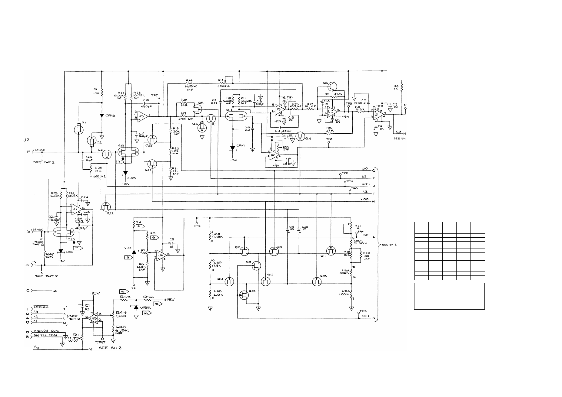
Figure 8-1. A1 Main PCB Assembly (cont)
8-3