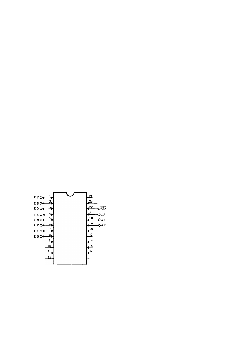
Mz3500, Clkoo out 0, Gateoo gndo – Sharp MZ-3500 User Manual
Page 69
Attention! The text in this document has been recognized automatically. To view the original document, you can use the "Original mode".

MZ3500
D0-D7
Data Bas
RXD
Receive Data (IN/OUT)
WR
Write (IN)
RD
Read (IN)
C/D
Control/Data (IN/OUT)
D7 ' DO
CS
Chip Select (IN)
DSR
Data Set Ready (IN)
DTR
Data Terminal Ready (OUT)
RTS
Request to Send (OUT)
CTS
Clear to Send (IN)
TXRDY
. Transmitter Ready (OUT)
TXC
Transmitter Clock (IN)
AO
TXE
. Transmitter Empty (OUT)
A1
RXC
. Receiver Clock (IN)
SYNET/BD
: SYNC Detect/Break Detect (IN/OUT)
CS
Block diagram
2) UPD8253C-5 (Programmable Interval Timer)
The UPD8253-5 is a programmable counter/timer speci
fically
designed
for
the
8
-bit
microcomputer
system.
It consists of three sets of 16-bit counters that operate
under a maximum counter rate of 4MHz. Timer and six
operational modes are programmed to be used for a wide
range of microcomputer system timing control.
Features
• Z-80 compatible
• Three sets of 16-bit counters
•
DC-4MHZ of count rate
•
Programmable six operational modes and timer
duration
• Choice of binary counter/BCD counter
•
N-channel MOS, input/output TTL compatible
• Single -t5V supply, 24-pin DIP
•
Intel 8253-5 compatible
Pin configuration (Top View)
CLKOO
OUT 0
04
GATEOO
GNDo
oVcc
OWR
OCLK2
>OOUT2
OGATE2
OCLKl
OGATE1
li—K)OUTl
A
—\ Data bus
\—^ buffer
/
Read/
write
logic
Control
word
register
Ico
Vr/
C=^
# 0
Counter ^ ------------- C I K O
<
------(,MhO
-►(n 1 0
Counter
# 1
^--------- Ci K 1
<--------- OAl h
-► ()l I 1
w
Counter
# 2
------ Cl h2
*
------ GAlt2
-►01 T2
D7~D0
Data Bus
(8
bit)
CLKN
Counter Clock Inputs
GATEN
Counter Gate Inputs
OUTN
Counter Outputs
RD
. Read Counter
WR
Write Command or Data
CS
Chip Select
A1~A0
: Counter Select
Vcc
. -1-5 Volts
GND
. Ground
76
