Sharp MZ-3500 User Manual
Page 32
Attention! The text in this document has been recognized automatically. To view the original document, you can use the "Original mode".

hi''
3«)0
CH48
O' For 40 digit display
1 : For 80 digit display
There is a 40/80 digit switching signal I/O port
in the gate array of CSP1 and CSP2, but, the I/O
signal called CH48 is provided apart from the I/O
port.
08/16 — I/O port inside CSP1 and CSP2.
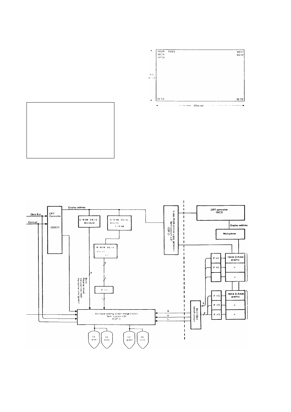
7) Graphic V RAM Address
Relation between VRAM address and screen (640 x 200 dors)
8-bit structure
Relation tretwepn VRAM address and screen
200
Uyte
0000 UOOI 0002 0003
UU )i
0050 0051
00\0
OOFO
3F30
31 7)
Graphic
address
map for
200 rasters
16-bit structure
Graphic
address
map for
400 rasters
CRTC block diagram
Color graphic VRAM PWB (option)
'iBK
byte
(option I)
48K
byte
(option tl)
