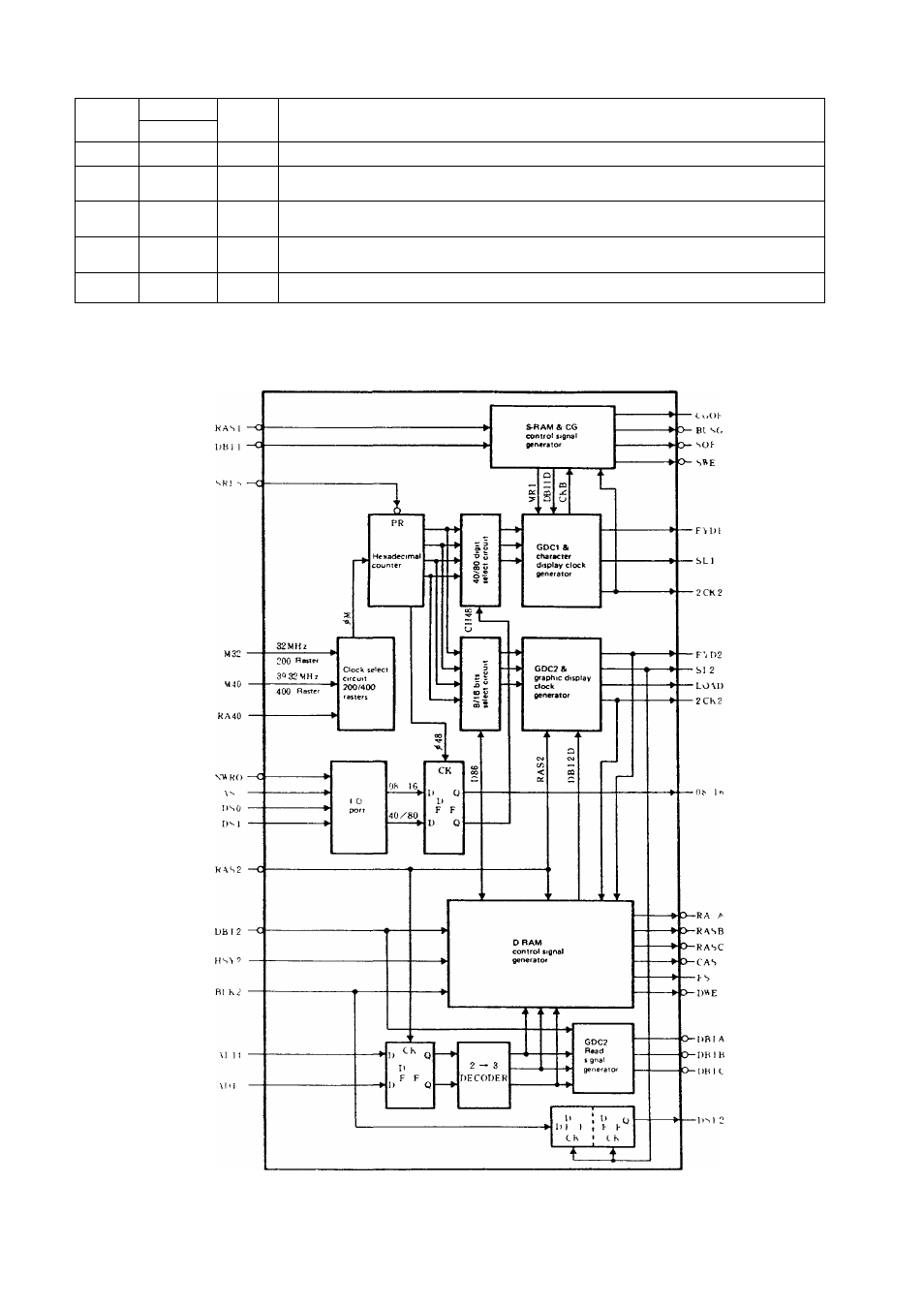
Csp 2 block diagram – Sharp MZ-3500 User Manual
Page 37
Attention! The text in this document has been recognized automatically. To view the original document, you can use the "Original mode".

M/3^.00
Pm No
Prior lly
IN/OUT
Function
Signal Name
36
M32
IN
Clock input 32MHz, 200 raster
37
FS
OUT
Graphic DRAM address multiplexer signal (High order 8 bits (ADS AD1 5] /low o''der S
(ADO AD7] select signal )
38
DSP2
OUT
Display timing signal (In the CSP
2.
the signal BLINK from GDC2 is delayed by 2 collor intervals to
create this signal )
39
2
OUT
Graphic D RAM CAS (COLUMN ADDRESS SELECT) signal
(Line address selection)
40
Vcc
IN
+ 5V supply
CSP 2 Block Diagram
42 -
