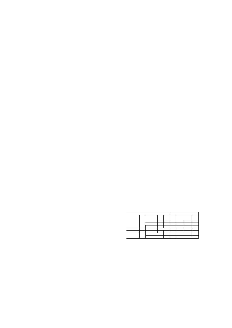
M/3s00, Hex dhus, El) fe ff – Sharp MZ-3500 User Manual
Page 20: Do d7 do 1)7, Do d7 d6, I i ski s msi mso ma2 mai mao m02 mol moo, S'\2, Sec fd3 fd2 edi skdy sack 1 np2, 1 npo mf2, Signal
Attention! The text in this document has been recognized automatically. To view the original document, you can use the "Original mode".

M/3S00
MAIN CPU
I/O PORT IN MEMORY MAPPER
ADDKKSS
-\7 A6 A5 A4 A3 A2 Al AO
1 1 1 1 1 0 0
1 1 1 1 1 1 0 1
1 1 1 1 1 1 1 0
1 1 1 1 1 1 1 1
HEX DHUS
E C
El)
FE
FF
D I
DO
D7
DO
1)7
U 6
D5
D4
D2
D1
DO
D4
D3
D2
D1
DO
D7
D6
D5
1)4
D3
D2
U 1
DO
D7
D6
1 ( )
OUT
OUT
IN
IN
OUT
SKUH
I I
SKI s
MSI
MSO
MA2
MAI
MAO
M02
MOl
MOO
S\\4
S\)3
S'\2
Stt 1
SEC
FD3
FD2
EDI
SKDY
SACK
1 NP2
INPl
1 NPO
MF2
ME 1
SRQ Bus request from the main CPU to the sub-CPU
Sub-CPU reset signal
Memory system define
Bank select signal to memory area of COOO-FFFF.
Bank select signal to memory area of 2000-3FFF.
System assign switch
FD assign
t. ^
------------------------------------------
TÌ
1
Sub-CPU READY
signal
V
Sub-CPU
acknowledge signal
Interrupt status
(SW8)
#1
1. All output signals are reset to low level upon power on,
' except for SRBQ that goes high.
2. Noted with a star mark "A" are input/output signals, and
rest of others are processed in the LSI.
#1 I/O port output of MEI and ME2 uses the memory at
the addresses.
( ME2-^8000~ BFFF
1 MEI ^4000 ~7FFF
_____
When MEI and ME2 are in high state, RSAB (RASA) is
inhibited
during
memory
addresses
in
RAM-A
that
correspond
to
overlayed
addresses
for
ME!
and
ME2
This is not true during SDÌ mode.
‘ VK IN MEMCKT MM I Mf
'
M I
TO ENCODMf
< * n r i T
M(t»M FNCODFK
MFH
noh
IMP 112h
ii3h
1T4H
IM 2
—
IM «
IMH
1 T s T T i T
IMI
IN=Tt INF?
JNT3
INT4
T v f
, X 1
'I
X X
X
X
1
1
L
1 H
f " ÌL
t
T“
X X
X
X
X
X
tl
1
X X
1
H
L
1
"
i
"
M
1 X
1
H
L
” -J
H
, " 1 '
X
L
H
H
L
II
H M
>-
X
H
■ ^ ■
1
H
H H
H
L
H
L
X
FkoM SI Ml
I h <• 11
Wait timing generator
WAIT IS issued once per main CPU fetch cycle.
Its outui IS tri state
TO MAIN Cl I
- 23 -
