Pdr-04, Pin function – Pioneer PDR-04 User Manual
Page 93
Attention! The text in this document has been recognized automatically. To view the original document, you can use the "Original mode".
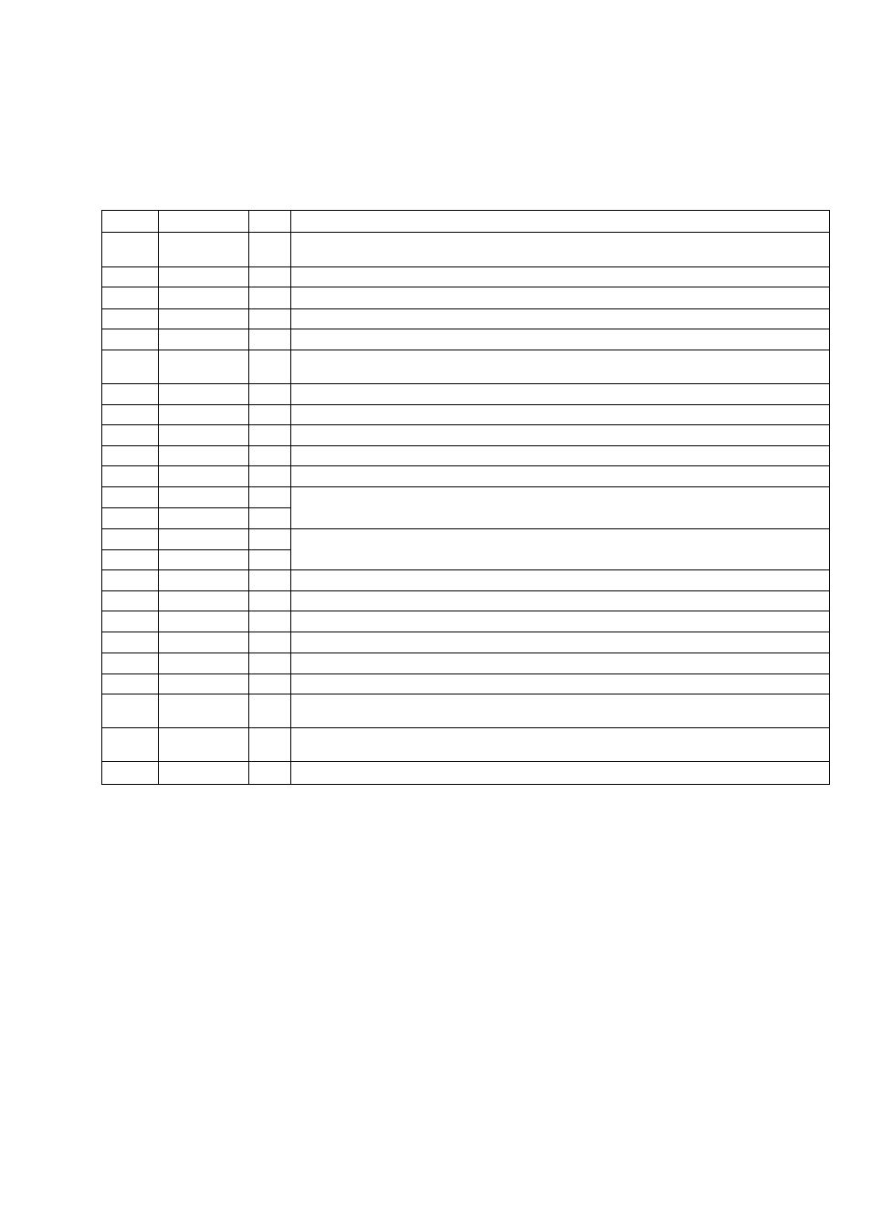
Pin Function
PDR-04
Pin No.
Pin Name
I/O
Function
1
CKS
1
Clock selection At normal speed ; L : XTI= 256fs, H : XTI= 384fs
At double speed ; L: XTI= 128fs , H : XTI= 192fs
2
DVDD
-
Digital power supply
3
DVSS
-
Digital ground
4
XTO
0
Crystal resonator output
5
XTI
1
Clock input
6
PD
1
Power down
When this pin is set to L, reset the filter and modulator, and it becomes power down state.
7
BICK
1
Serial bit clock 64fs is recommended.
8
SDATA
1
Serial data Input 2's complement, MSB first
9
LRCK
1
UR clock
10
SMUTE
1
Soft mute H: start the soft mute L: release
11
DFS
1
Double speed sampling mode L: Normal speed H: Double speed
12
DEMO
1
Deemphasis mode
13
DEMI
1
It correspond to tri-frequency
14
DIPO
1
Input format
15
DIPI
1
16
BVDD
-
Power supply
17
AOUTR
0
R ch analog output
18
AOUTL
0
L ch analog output
19
VCOM
0
Common voltage pin, AVDD/2
20
AVDD
-
Analog power supply
21
AVSS
Analog ground
22
VREP
1
Reference voltage input
The voltage difference between this pin and AVSS pin decide to full scale of D/A output.
23
DZP
0
Zero Input detection pin When the data is input to SDATA pin which is continuosly zero for 8192
times on both channels, this pin becomes "H".
24
TTL
I
I/F level selection T": CMOS level (DVDD= 2.7V to 5.5V) "H": TTL level (DVDD= 4.5V to 5.5V)
93