Connecting to an external device, How to connect, I/o circuit diagram – KEYENCE DL-RB1A User Manual
Page 3: Output settings, 3connecting to an external device
3
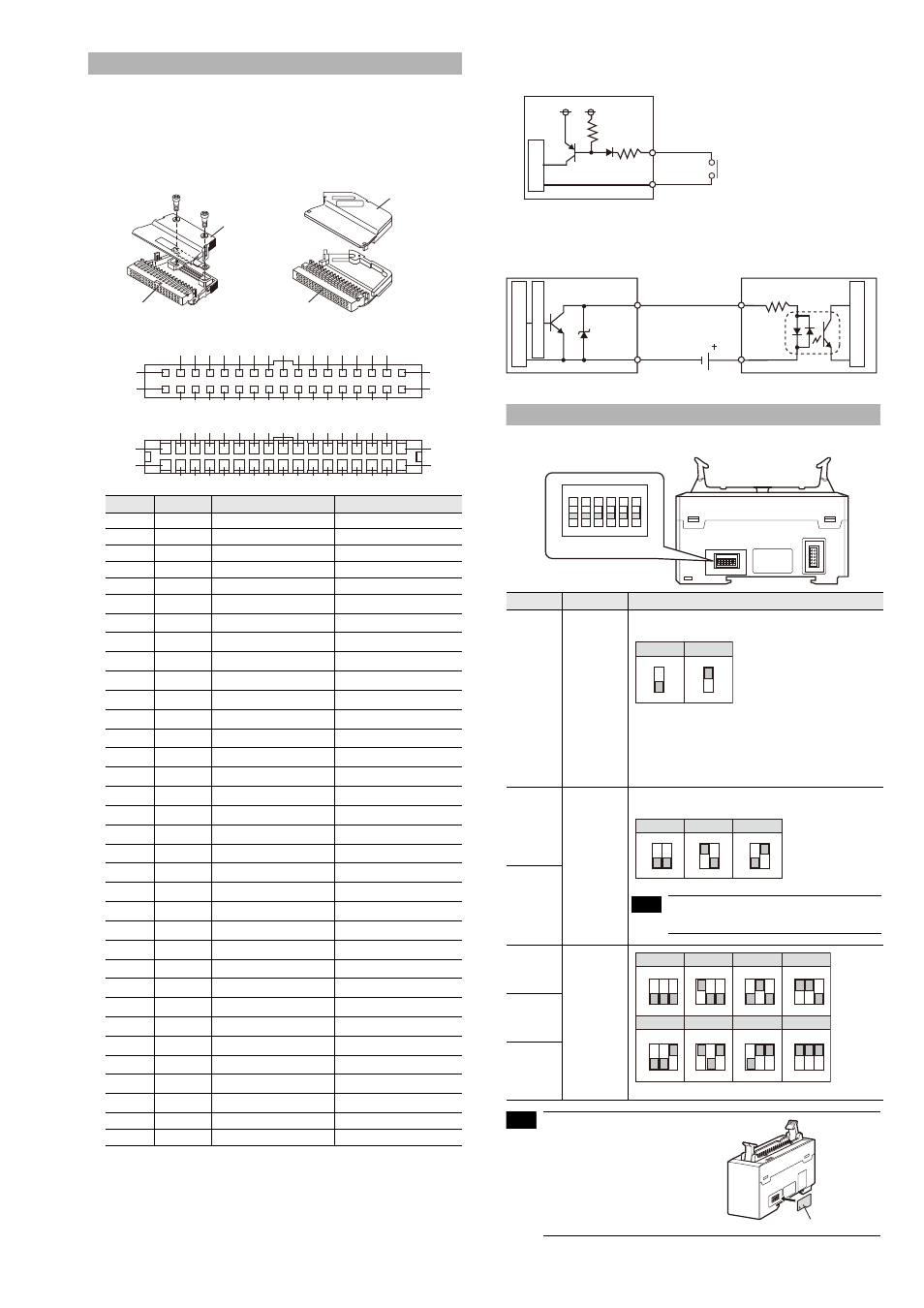
Connecting to an External Device
How to connect
To connect BCD Output Unit DL-RB1A to an external device, use the
connector (MIL connector, female, 34-pin) shown below.
Pin arrangement of I/O connector
*1 Be sure to load the BCD output (Pin No. 6 to 30) when the strobe
output (Pin No. 31) becomes ON. Refer to the "BCD Output Unit
DL-RB1A User's Manual" for more details about the strobe output.
*2 Alarm output will be turned OFF when the alarm is generated.
(ON in normal condition)
I/O circuit diagram
Input circuit diagram (Pin No. 1 to 5)
* Pin No. 33 and 34 are common to the 0V blue wire on the main sensor amplifier.
Output circuit (Pin No. 6 to 32)
* Pin No. 33 and 34 are common to the 0V blue wire on the main sensor amplifier.
Output Settings
Use the advanced setting switch for output settings.
• After changing the
settings, be sure to
cycle power.
• After setting, reattach
the included switch
protection sticker.
Pin No.
Direction
Signal name
Description
1
Input
IDSEL1
ID No. selection input 1
2
Input
IDSEL2
ID No. selection input 2
3
Input
IDSEL3
ID No. selection input 3
4
Input
IDSEL4
ID No. selection input 4
5
Input
DRQ
Data request input
6
Output
BCD DIGIT 1 (1)
BCD 1st digit 1 x 10
0
7
Output
BCD DIGIT 1 (2)
BCD 1st digit 2 x 10
0
8
Output
BCD DIGIT 1 (4)
BCD 1st digit 4 x 10
0
9
Output
BCD DIGIT 1 (8)
BCD 1st digit 8 x 10
0
10
Output
BCD DIGIT 2 (1)
BCD 2nd digit 1 x 10
1
11
Output
BCD DIGIT 2 (2)
BCD 2nd digit 2 x 10
1
12
Output
BCD DIGIT 2 (4)
BCD 2nd digit 4 x 10
1
13
Output
BCD DIGIT 2 (8)
BCD 2nd digit 8 x 10
1
14
Output
BCD DIGIT 3 (1)
BCD 3rd digit 1 x 10
2
15
Output
BCD DIGIT 3 (2)
BCD 3rd digit 2 x 10
2
16
Output
BCD DIGIT 3 (4)
BCD 3rd digit 4 x 10
2
17
Output
BCD DIGIT 3 (8)
BCD 3rd digit 8 x 10
2
18
Output
BCD DIGIT 4 (1)
BCD 4th digit 1 x 10
3
19
Output
BCD DIGIT 4 (2)
BCD 4th digit 2 x 10
3
20
Output
BCD DIGIT 4 (4)
BCD 4th digit 4 x 10
3
21
Output
BCD DIGIT 4 (8)
BCD 4th digit 8 x 10
3
22
Output
BCD DIGIT 5 (1)
BCD 5th digit 1 x 10
4
23
Output
BCD DIGIT 5 (2)
BCD 5th digit 2 x 10
4
24
Output
BCD DIGIT 5 (4)
BCD 5th digit 4 x 10
4
25
Output
BCD DIGIT 5 (8)
BCD 5th digit 8 x 10
4
26
Output
BCD DIGIT 6 (1)
BCD 6th digit 1 x 10
5
27
Output
BCD DIGIT 6 (2)
BCD 6th digit 2 x 10
5
28
Output
BCD DIGIT 6 (4)
BCD 6th digit 4 x 10
5
29
Output
BCD DIGIT 6 (8)
BCD 6th digit 8 x 10
5
30
Output
BCD SIGN
BCD data polarity code
31
Output
BCD STB
*1
Strobe output
32
Output
ALARM
*2
Alarm output
33
Common
COM
Common
34
Common
COM
Common
Housing
Housing
34-pin MIL connector set
OP-23139
34-pin MIL Slim connector set
OP-42224
Hood cover
Hood cover
4
1
2
3
5
7
9
11
13
15
17
19
21
23
25
27
29
31
6
8
10
12
14
16
18
20
22
24
26
28
30
32
33
34
33
34
1
2
4
3
5
7
9
11
13
15
17
19
21
23
25
27
29
31
6
12
10
8
14
20
18
16
22
28
26
24
30
32
▼ Mark
Mark
▼
Rear
Front
Switch No. Setting item
Combination
1
Output logic
Setting enabled only for BCD output (Pin No. 6 to
29) and BCD polarity code output (Pin No. 30).
* Settings before shipment.
Negative logic: Bit of an input device (external device
including PLC) will be 1 when the BCD
output (Pin No. 6 to 30) is ON.
Positive logic:
Bit of an input device (external device
including PLC) will be 1 when the BCD
output (Pin No. 6 to 30) is OFF.
2
BCD data
output
method
Set the BCD data output method except alarm
output (Pin No. 6 to 31).
* Settings before shipment.
Do not use the switches No.2 and 3 in
combinations other than those shown above.
3
4
BCD output
update
cycle in the
TIMER
mode
* Settings before shipment.
5
6
Main circuit
(Short-circuit current 1mA max.)
+5V
1 to 5
33 or 34*
6 to 32
33 or 34*
IN
COM
Photo coupler insulation
PLC etc.
Inter
nal circuit
Inter
nal circuit
Ov
er current protect circuit
10
0
N
2 3 4 5 6
6
10 2
N
3 4 5 6
Advanced setting switch
ON
1
ON
1
Negative logic * Positive logic
ON
2 3
ON
2 3
ON
2 3
OUT mode* OR mode TIMER mode
Note
ON
ON
ON
ON
4 5 6
ON
ON
ON
ON
4 5 6
4 5 6
4 5 6
4 5 6
4 5 6
4 5 6
4 5 6
1ms
*
2ms
4ms
8ms
16ms
32ms
64ms
128ms
Note
Switch protection sticker