4 display connector (internal), 1 lvds flat panel connector (lvds) (j20), Display connector (internal) – Kontron KTHM65-mITX User Manual
Page 39: Lvds flat panel connector (lvds) (j20), Internal connectors
KTHM65 Users Guide
KTD-N0838-A Page 39
5.4 Display connector (Internal)
The KTHM65 provides LVDS display connector.
For IO Area Display Connectors (DVI-I and two DP’s), see earlier section.
Two graphic pipes are supported; meaning that up to two independent displays can be implemented
using any two of display connectors (IO Area - and Internal connectors).
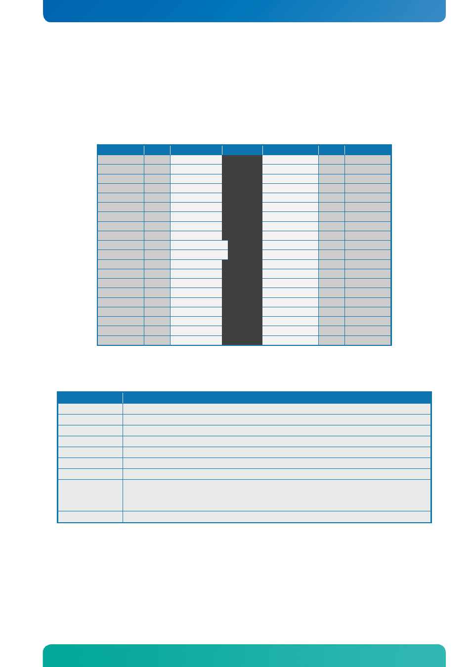
5.4.1 LVDS Flat Panel Connector (LVDS) (J20)
Note
Type
Signal
PIN
Signal
Type
Note
Max. 0.5A PWR
+12V
1 2
+12V
PWR Max. 0.5A
Max. 0.5A PWR
+12V
3 4
+12V
PWR Max. 0.5A
Max. 0.5A PWR
+12V
5 6
GND
PWR Max. 0.5A
Max. 0.5A PWR
+5V
7 8
GND
PWR Max. 0.5A
Max. 0.5A PWR
LCDVCC
9 10
LCDVCC
PWR Max. 0.5A
2K2Ω, 3.3V OT
DDC CLK
11 12
DDC DATA
OT 2K2Ω, 3.3V
3.3V level
OT
BKLTCTL
13 14
VDD ENABLE OT 3.3V level
3.3V level
OT
BKLTEN#
15 16
GND
PWR Max. 0.5A
LVDS LVDS A0-
17 18
LVDS A0+ LVDS
LVDS LVDS A1-
19 20
LVDS A1+ LVDS
LVDS LVDS A2-
21 22
LVDS A2+ LVDS
LVDS LVDS ACLK-
23 24
LVDS ACLK+ LVDS
LVDS LVDS A3-
25 26
LVDS A3+ LVDS
Max. 0.5A PWR
GND
27 28
GND
PWR Max. 0.5A
LVDS LVDS B0-
29 30
LVDS B0+ LVDS
LVDS LVDS B1-
31 32
LVDS B1+ LVDS
LVDS LVDS B2-
33 34
LVDS B2+ LVDS
LVDS LVDS BCLK-
35 36
LVDS BCLK+ LVDS
LVDS LVDS B3-
37 38
LVDS B3+ LVDS
Max. 0.5A PWR
GND
39 40
GND
PWR Max. 0.5A
Note: The KTHM65 on-board LVDS connector supports single and dual channel, 18/24bit SPWG
panels up to the resolution 1600x1200 or 1920x1080 and with limited frame rate some
1920x1200.
Signal
Description
LVDS A0..A3
LVDS A Channel data
LVDS ACLK
LVDS A Channel clock
LVDS B0..B3
LVDS B Channel data
LVDS BCLK
LVDS B Channel clock
BKLTCTL
Backlight control (1), PWM signal to implement voltage in the range 0-3.3V
BKLTEN#
Backlight Enable signal (active low) (2)
VDD ENABLE Output Display Enable.
LCDVCC
VCC supply to the display. Power-on/off sequencing depending on selected (in BIOS
setup) display type. 5V or 3.3V selected in BIOS setup. LCDVCC is shared with eDP
connector. Maximum load is 1A at both voltages.
DDC CLK
DDC Channel Clock
Notes: Windows API will be available to operate the BKLTCTL signal. Some Inverters have a limited
voltage range 0- 2.5V for this signal: If voltage is > 2.5V the Inverter might latch up. Some
Inverters generates noise on the BKLTCTL signal, resulting in making the LVDS transmission
failing (corrupted picture on the display). By adding a 1Kohm resistor in series with this signal,
mounted in the Inverter end of the cable kit, the noise is limited and the picture is stable.
If the Backlight Enable is required to be active high then, check the following BIOS Chipset
setting: Backlight Signal Inversion = Enabled.
Internal Connectors