Elecraft KXB3080 User Manual
Page 19

19
LPF1 Module
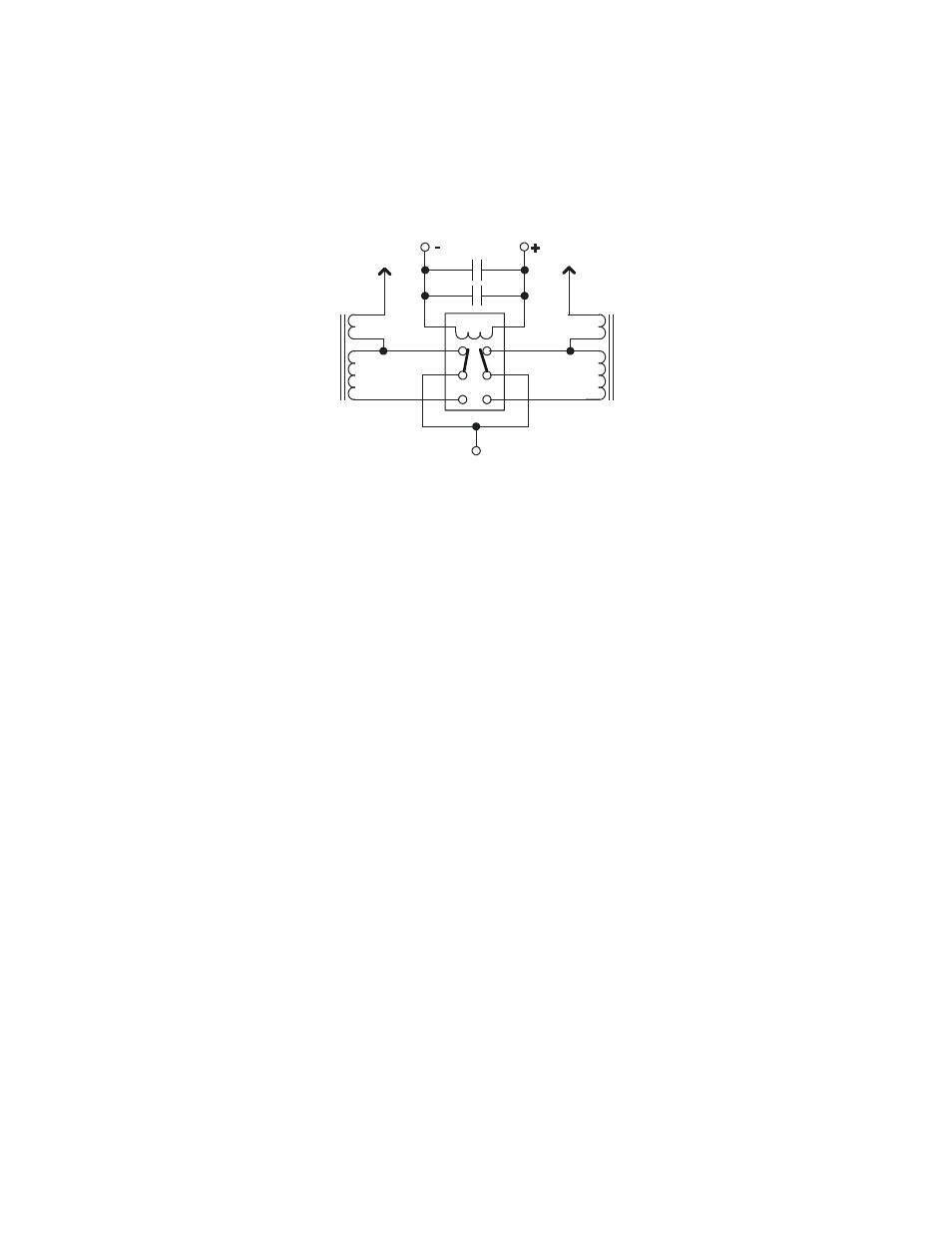
The low-pass filter module adds 80 meter coverage to the filter network at the output of the transmitter by
replacing the two inductors in the original circuit with four inductors and an additional capacitor that are
switched in as required (see Figure 16). Relay K1 selects one of two windings on L1 and L2. On 40, 30,
and 20 meters, the smaller winding is selected. This corresponds to the OFF position of the relay, resulting
in zero added current drain on these bands. On 80 meters, K1 is turned ON via 5 volts from point F on the
KXB3080 module. This selects the larger winding on each of L1 and L2, moving the low-pass filter knee
down to about 4 MHz. Current drain increases by about 15 mA on 80 meters because K1 is a conventional
relay.
3
3
4
1
2
L1
2
43
7
56
8
1
+
+
K1
4
1
2
L2
COMMON
X
Y
C1
C9
1-2: Green
3-4: Red
-
NOTE: "+" and "-" labels are reversed on Rev A LPF1 board.
Figure 16. LPF1 Module Schematic Diagram.
KXB3080 Module
A schematic diagram of the KXB3080 module is shown in Figure 17. When the KX1 is switched to 30
meters (or tuned below about 6.7 MHz on 40 meters), the MCU places 5 volts DC on point D, forward
biasing the associated diode of dual PIN diodes D1 and D2. This inserts the series combination of C3/C4 in
parallel with points A and B, i.e. in parallel with CA on the KX1; it also inserts C1 from point C to RF
ground, or across L7 on the KX1. At other times point D is at 0 volts, reverse biasing the diodes so they
have a minimal effect on the band-pass filter.
When the rig is switched to 80 meters, the MCU places 0 volts on point E. This turns on Q1, placing 5 volts
at its collector. This turns on the other half of D1 and D2, inserting C2 and C5 into the tuned circuits to re-
resonate them at approximately 3.6 MHz. At the same time, 5 volts appears on point F to turn on the low-
pass filter relay (on the LPF1 module). D3 protects Q1 from inductive kickback by the relay.
Q1 is needed because the signal at point E cannot drive PIN diodes or the relay directly. The associated
MCU pin is also used as the SPI-bus clock, for communication with the DDS IC. R8 and C9 filter out the
short duty-cycle clock pulses that occur as you tune the VFO. Firmware sets the idling state of the SPI
clock signal based on whether or not 80 meters is selected, and this is the state that appears at the collector
of Q1.
