Switching characteristics, Thermal resistance – Cypress CY7C1312AV18 User Manual
Page 10

CY7C1310AV18
CY7C1312AV18
CY7C1314AV18
PRELIMINARY
Document #: 38-05497 Rev. *A
Page 10 of 21
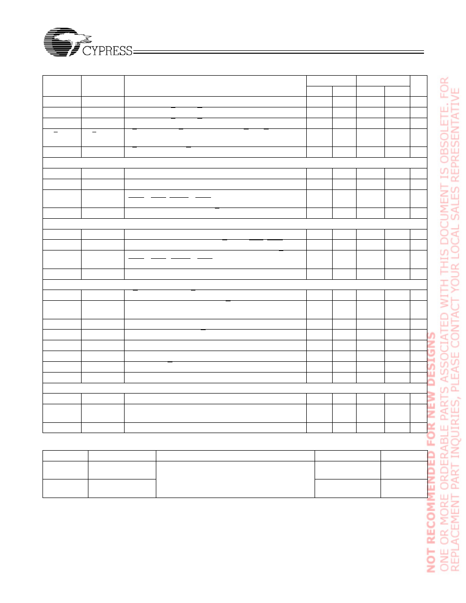
Switching Characteristics
Over the Operating Range
[16,17]
Cypress
Consortium
Description
167 MHz
133 MHz
Unit
Parameter Parameter
Min.
Max.
Min.
Max.
t
CYC
t
KHKH
K Clock and C Clock Cycle Time
6.0
7.9
7.5
8.4
ns
t
KH
t
KHKL
Input Clock (K/K and C/C) HIGH
2.4
–
3.0
–
ns
t
KL
t
KLKH
Input Clock (K/K and C/C) LOW
2.4
–
3.0
–
ns
t
KHKH
t
KHKH
K/K Clock Rise to K/K Clock Rise and C/C to C/C Rise (rising
edge to rising edge)
2.7
–
3.38
–
ns
t
KHCH
t
KHCH
K/K Clock Rise to C/C Clock Rise (rising edge to rising edge)
0.0
2.8
0.0
3.55
ns
Set-up Times
t
SA
t
SA
Address Set-up to K Clock Rise
0.5
–
0.5
–
ns
t
SC
t
SC
Control Set-up to Clock (K, K) Rise (RPS, WPS)
0.5
–
0.5
–
ns
t
SCDDR
t
SC
Double Data Rate Control Set-up to Clock (K, K) Rise
(BWS
0
, BWS
1
, BWS
3
, BWS
4
)
0.5
–
0.5
–
ns
t
SD
t
SD
D
[X:0]
Set-up to Clock (K and K) Rise
0.5
–
0.5
–
ns
Hold Times
t
HA
t
HA
Address Hold after Clock (K and K) Rise
0.5
–
0.5
–
ns
t
HC
t
HC
Control Hold after Clock (K and K) Rise (RPS, WPS)
0.5
–
0.5
–
ns
t
HCDDR
t
HC
Double Data Rate Control Hold after Clock (K and K) Rise
(BWS
0
, BWS
1
, BWS
3
, BWS
4
)
0.5
–
0.5
–
ns
t
HD
t
HD
D
[X:0]
Hold after Clock (K and K) Rise
0.5
–
0.5
–
ns
Output Times
t
CO
t
CHQV
C/C Clock Rise (or K/K in Single Clock Mode) to Data Valid
–
0.50
–
0.50
ns
t
DOH
t
CHQX
Data Output Hold after Output C/C Clock Rise (Active to
Active)
–0.50
–
–0.50
–
ns
t
CCQO
t
CHCQV
C/C Clock Rise to Echo Clock Valid
–
0.50
–
0.50
ns
t
CQOH
t
CHCQX
Echo Clock Hold after C/C Clock Rise
–0.50
–
–0.50
–
ns
t
CQD
t
CQHQV
Echo Clock High to Data Valid
–
0.40
–
0.40
ns
t
CQDOH
t
CQHQX
Echo Clock High to Data Invalid
–0.40
–
–0.40
–
ns
t
CHZ
t
CHZ
Clock (C and C) Rise to High-Z (Active to High-Z)
[18,19]
–
0.50
–
0.50
ns
t
CLZ
t
CLZ
Clock (C and C) Rise to Low-Z
[18,19]
–0.50
–
–0.50
–
ns
DLL Timing
t
KC Var
t
KC Var
Clock Phase Jitter
–
0.20
–
0.20
ns
t
KC lock
t
KC lock
DLL Lock Time (K, C)
1024
–
1024
-
cycl
es
t
KC Reset
t
KC Reset
K Static to DLL Reset
30
30
ns
Thermal Resistance
[20]
Parameter
Description
Test Conditions
165 FBGAPackage
Unit
Θ
JA
Thermal Resistance
(Junction to Ambient)
Test conditions follow standard test methods and
procedures for measuring thermal impedence, per
EIA / JESD51.
16.7
°C/W
Θ
JC
Thermal Resistance
(Junction to Case)
2.5
°C/W
Notes:
16. All devices can operate at clock frequencies as low as 119 MHz. When a part with a maximum frequency above 133 MHz is operating at a lower clock frequncy,
it requires the input timings of the frequency range in which it is being operated and will output data with the output timings of that frequency range.
17. Unless otherwise noted, test conditions assume signal transition time of 2V/ns, timing reference levels of 0.75V, Vref = 0.75V, RQ = 250
Ω, V
DDQ
= 1.5V, input
pulse levels of 0.25V to 1.25V, and output loading of the specified I
OL
/I
OH
and load capacitance shown in (a) of AC test loads.
18. t
CHZ
, t
CLZ
, are specified with a load capacitance of 5 pF as in part (b) of AC Test Loads. Transition is measured
± 100 mV from steady-state voltage.
19. At any given voltage and temperature t
CHZ
is less than t
CLZ
and t
CHZ
less than t
CO
.
