Specifications – Rockwell Automation 1771-OFE Analog Output Module Installation Instructions User Manual
Page 16
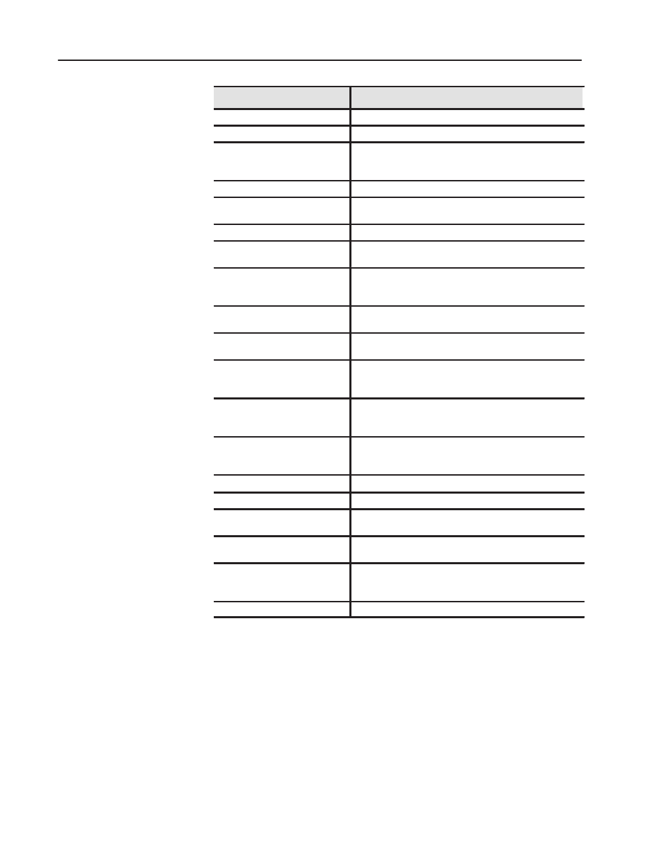
Analog Output Module
16
Publication 1771-IN044C-EN-P - October 2002
Description
Value
Outputs per Module
4 Individually Isolated
Module Location
Bulletin 1771 I/O Chassis - One Slot
Output Voltage Ranges (Nominal) -
1771ĆOFE1
+1 to +5V DC
-10 to +10V DC
0 to +10V DC
Output Current (maximum)
10mA per Channel in Voltage Mode (1771-OFE1)
Output Current Ranges (Nominal)
+4 to +20mA, 5V dc (1771-OFE2)
0 to +50mA, 12.5V dc (1771-OFE3)
Digital Resolution
12ĆBit Binary - 1 Part in 4095
Output Capacitance
0.01
µ
F (Voltage Outputs)
0.022
µ
F (Current Outputs)
Output Impedance
<0.25 ohms for Voltage Outputs Exclusive of Contact Wiring
Resistance
>1.5 megohms for Current Outputs
Max Loop Impedance in the
Current Mode
1771ĆOFE2 - Up to 1200 ohms Load Resistance
1771ĆOFE3 - Up to 400 ohms Load Resistance
Output Overload Protection
All outputs are protected against short circuit load conditions
not to exceed one minute.
Backplane Power
1771ĆOFE1 - 1.50A
1771ĆOFE2 - 1.50A
1771ĆOFE3 - 2.50A
Power Dissipation
1771ĆOFE1 - 7.9W
1771ĆOFE2 - 7.9W
1771ĆOFE3 - 13.1W
Thermal Dissipation
1771ĆOFE1 - 26.9 BTU/hr
1771ĆOFE2 - 26.9 BTU/hr
1771ĆOFE3 - 44.5 BTU/hr
Adjacent Slot Power Dissipation
10 Watts (max.)
Isolation Voltage
Tested to 850V dc for 1s
D/A Converter Specifications
Settling Time
0.8 ms Maximum for a Resistive Load
Internal Scan Rate
8.0 ms for All Channels Using BCD Data and Scaling 1.6 ms
for All Channels Using Binary Data and No Scaling
Accuracy (Including Linearity, Gain,
and Offset at 25
o
C)
+0.1% of Full Scale
+1/2 LSD (BCD Mode)
+1/2 LSB (BINARY Mode)
Temperature Coefficient
+50 ppm/
o
C of Full Scale Range
Specifications