Cirrus Logic EP7312 User Manual
Page 42
42
Copyright Cirrus Logic, Inc. 2011
(All Rights Reserved)
DS508F2
EP7312
High-Performance, Low-Power System on Chip
F13
nBATCHG
I
Battery changed sense input
F14
VSSIO
Pad ground
I/O ground
F15
D[11]
1
Low
I/O
Data I/O
F16
VDDIO
Pad power
Digital I/O power, 3.3V
G1 PB[1]
1
Input
‡
I
GPIO port B
G2
VDDIO
Pad power
Digital I/O power, 3.3V
G3
TDO
1
Input
‡
O
JTAG data out
G4 PB[4]
1
Input
‡
I
GPIO port B
G5 PB[6]
1
Input
‡
I
GPIO port B
G6
VSSCore
Core ground
Core ground
G7
VSSRTC
RTC ground
Real time clock ground
G8
DD[0]
1
Low
O
LCD serial display data
G9 D[3]
1
Low
I/O
Data
I/O
G10
VSSRTC
RTC ground
Real time clock ground
G11
A[7]
1
Low
O
System byte address
G12
A[8]
1
Low
O
System byte address
G13
A[9]
1
Low
O
System byte address
G14
VSSIO
Pad ground
I/O ground
G15
D[12]
1
Low
I/O
Data I/O
G16
D[13]
1
Low
I/O
Data I/O
H1 PA[7]
1
Input
‡
I/O
GPIO port A
H2 PA[5]
1
Input
‡
I/O
GPIO port A
H3
VSSIO
Pad ground
I/O ground
H4 PA[4]
1
Input
‡
I/O
GPIO port A
H5 PA[6]
1
Input
‡
I/O
GPIO port A
H6 PB[0]
1
Input
‡
I/O
GPIO port B
H7 PB[2]
1
Input
‡
I/O
GPIO port B
H8
VSSRTC
RTC ground
Real time clock ground
H9
VSSRTC
RTC ground
Real time clock ground
H10
A[10]
1
Low
O
System byte address
H11
A[11]
1
Low
O
System byte address
H12
A[12]
1
Low
O
System byte address
H13
A[13]/DRA[14]
1
Low
O
System byte address / SDRAM address
H14
VSSIO
Pad ground
I/O ground
H15
D[14]
1
Low
I/O
Data I/O
H16
D[15]
1
Low
I/O
Data I/O
J1 PA[3]
1
Input
‡
I/O
GPIO port A
J2 PA[1]
1
Input
‡
I/O
GPIO port A
J3
VSSIO
Pad ground
I/O ground
J4 PA[2]
1
Input
‡
I/O
GPIO port A
J5 PA[0]
1
Input
‡
I/O
GPIO port A
J6
TXD[1]
1
High
O
UART 1 transmit data out
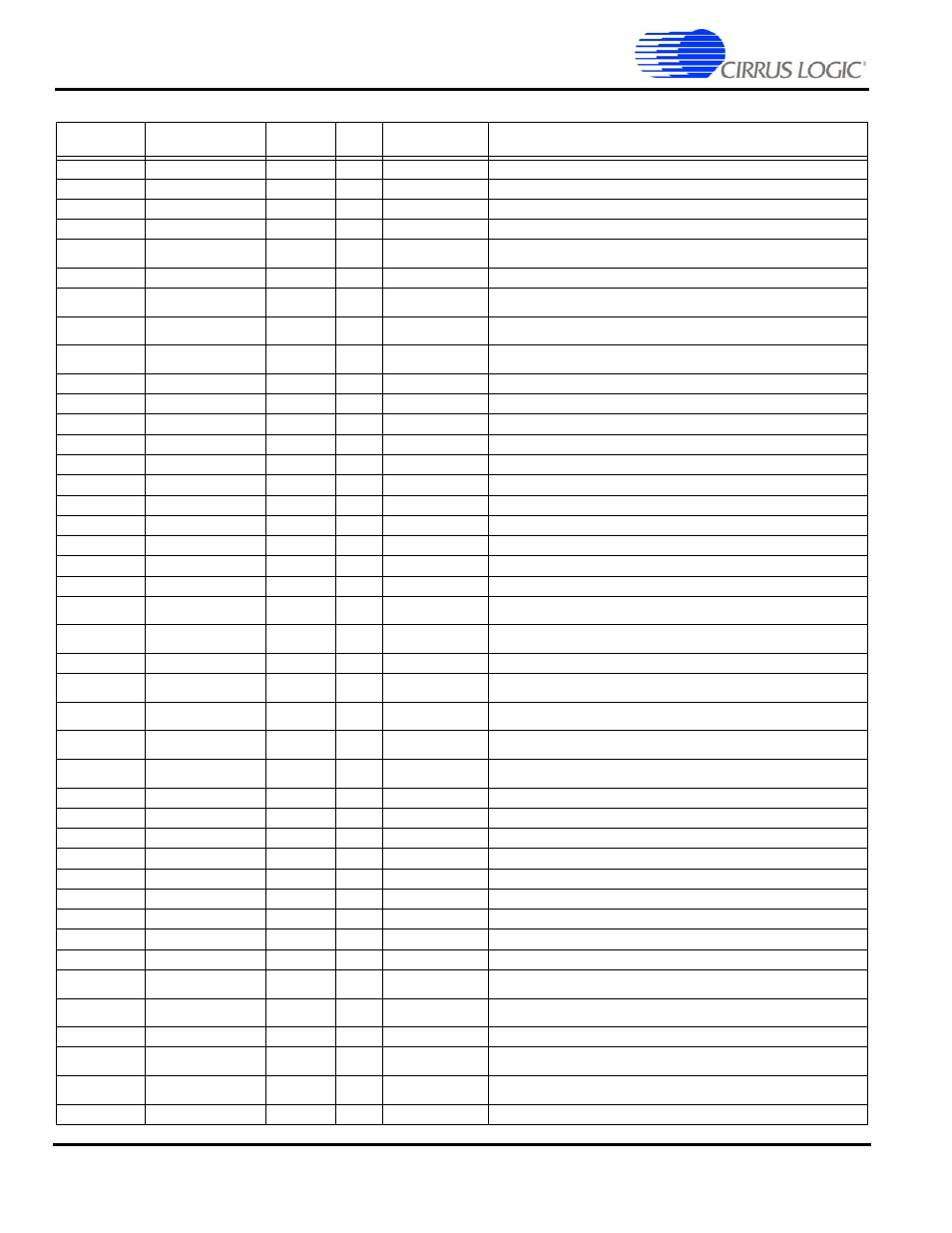
Table 21. 256-Ball PBGA Ball Listing (Continued)
Ball Location
Name
Strength
†
Reset
State
Type
Description