Timings, Timing diagram conventions, Timing conditions – Cirrus Logic EP7312 User Manual
Page 15: Timing diagram conventions timing conditions, Figure 2. legend for timing diagrams
DS508F2
Copyright Cirrus Logic, Inc. 2011
(All Rights Reserved)
15
EP7312
High-Performance, Low-Power System on Chip
Timings
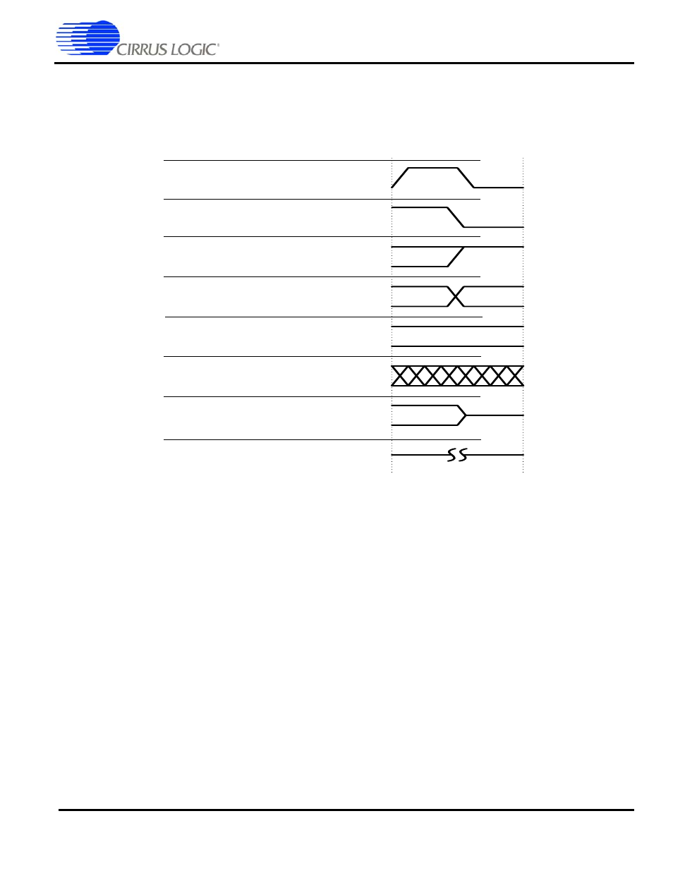
Timing Diagram Conventions
This data sheet contains timing diagrams. The following key explains the components used in these diagrams. Any variations are
clearly labelled when they occur. Therefore, no additional meaning should be attached unless specifically stated.
Timing Conditions
Unless specified otherwise, the following conditions are true for all timing measurements. All characteristics are specified at
V
DDIO
= 3.1 - 3.5 V and V
SS
= 0 V over an operating temperature of -40
C to +85C. Pin loadings is 50 pF. The timing values are
referenced to 1/2 V
DD
.
C l o c k
H i g h t o L o w
H i g h / L o w t o H i g h
B u s C h a n g e
B u s V a l i d
U n d e f i n e d / I n v a l i d
V a l i d B u s t o T r i s t a t e
B u s / S i g n a l O m i s s i o n
Figure 2. Legend for Timing Diagrams