Static memory burst write cycle – Cirrus Logic EP7312 User Manual
Page 25
DS508F2
Copyright Cirrus Logic, Inc. 2011
(All Rights Reserved)
25
EP7312
High-Performance, Low-Power System on Chip
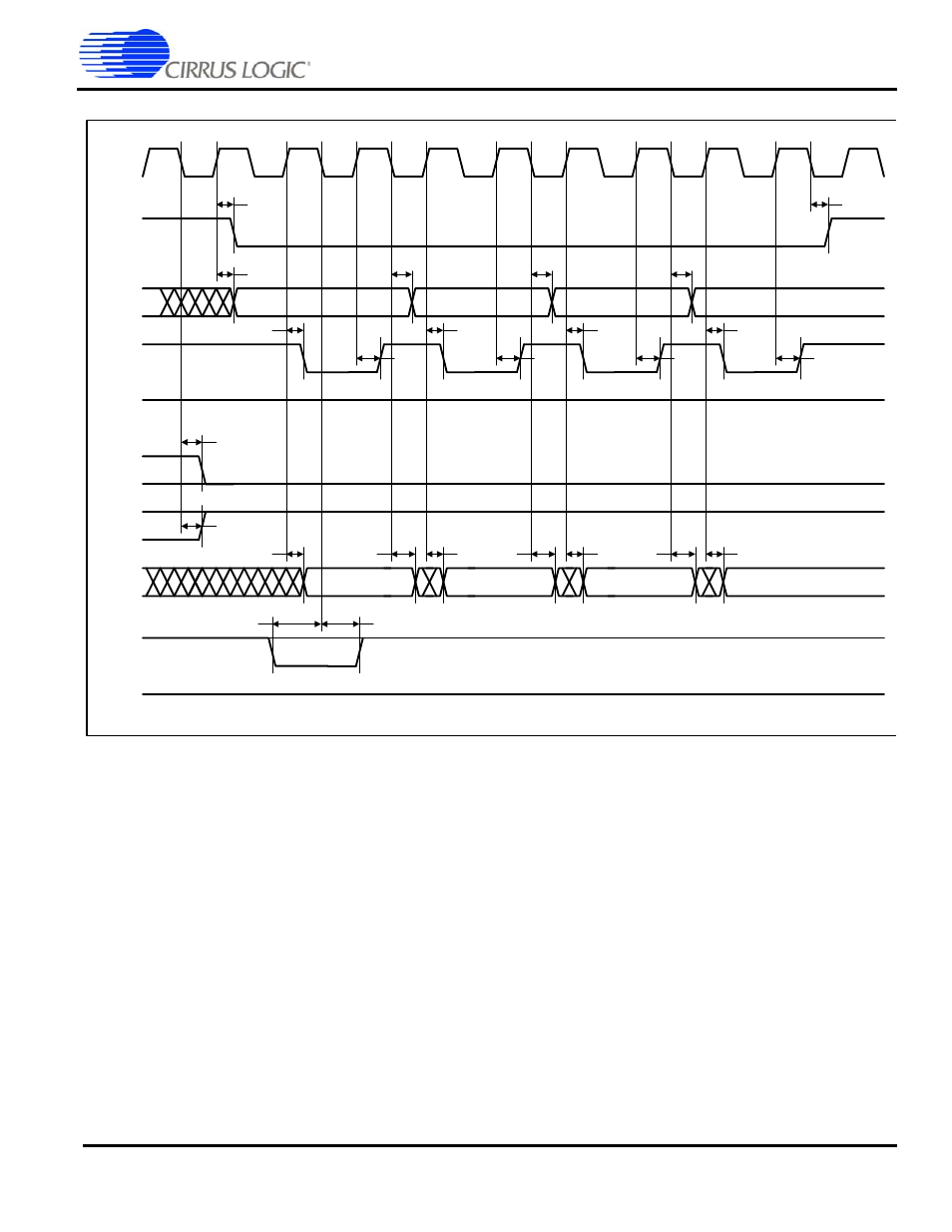
Static Memory Burst Write Cycle
Note:
1. Four cycles are shown in the above diagram (minimum wait states, 1-1-1-1). This is the maximum number of consecutive
cycles that can be driven. The number of consecutive cycles can be programmed from 2 to 4, inclusively.
2. The cycle time can be extended by integer multiples of the clock period (22 ns at 45 MHz, 27 ns at 36 MHz, 54 ns at
18.432 MHz, and 77 ns at 13 MHz), by either driving EXPRDY low and/or by programming a number of wait states. EXPRDY is
sampled on the falling edge of EXPCLK before the data transfer. If low at this point, the transfer is delayed by one clock period
where EXPRDY is sampled again. EXPCLK need not be referenced when driving EXPRDY, but is shown for clarity.
3. Zero wait states for sequential writes is not permitted for memory devices which use nMWE pin, as this cannot be driven with
valid timing under zero wait state conditions.
4. Address, Data, Halfword, Word, and Write hold state until next cycle.
EXPCLK
nCS
A
nMOE
HALF
WORD
WORD
D
nMWE
EXPRDY
WRITE
t
CSd
t
Ad
t
MWd
t
MWh
t
MWd
t
MWd
t
MWd
t
MWh
t
MWh
t
MWh
t
Ah
t
Ah
t
Ah
t
EXs
t
EXh
t
CSh
t
Dv
t
Dv
t
Dv
t
Dnv
t
Dnv
t
Dnv
t
Dv
t
HWd
t
WDd
Figure 10. Static Memory Burst Write Cycle Timing Measurement