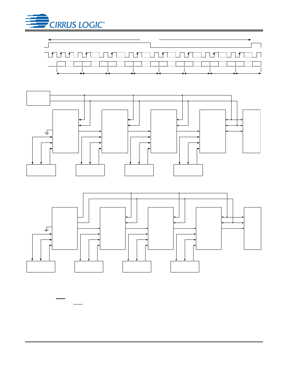
Figure 12. tdm master mode timing diagram, 5 reset, power-down, and start-up, Ured. see – Cirrus Logic CS8421 User Manual
Page 22: Reset, Figure 13, N in, Figure 14, Cs8421
22
DS641F6
CS8421
4.5
Reset, Power-Down, and Start-Up
When RST is low, the CS8421 enters a low-power mode, all internal states are reset, and the outputs are
disabled. After RST transitions from low to high, the part senses the resistor value on the configuration pins
(MS_SEL, SAIF, and SAOF) and sets the appropriate mode of operation. After the mode has been set (ap-
proximately 4
s), the part is set to normal operation and all outputs are functional.
OLRCK
OSCLK
LSB
MSB
LSB
MSB
LSB
MSB
LSB
MSB
LSB
MSB
LSB
MSB
SDOUT/
TDM_IN
SDOUT 3, ch A
32 clks
32 clks
32 clks
32 clks
32 clks
32 clks
LSB
MSB
LSB
MSB
32 clks
32 clks
SDOUT 3, ch B
SDOUT 2, ch A
SDOUT 2, ch B
SDOUT 1, ch A
SDOUT 1, ch B
SDOUT 4, ch A
SDOUT 4, ch B
256 OSCLKs
Figure 12. TDM Master Mode Timing Diagram
ILRCK
ISCLK
SDIN
OLRCK
OSCLK
SDOUT
TDM_IN
OLRCK
OSCLK
SDOUT
TDM_IN
ILRCK
ISCLK
SDIN
Output
Clock
Source
LRCK
SCLK
OLRCK
OSCLK
SDOUT
PCM Source 2
OLRCK
OSCLK
SDOUT
PCM Source 1
CS8421
1
Slave
CS8421
2
Slave
LRCK
SCLK
SDIN
DSP
Slave
OLRCK
OSCLK
SDOUT
TDM_IN
ILRCK
ISCLK
SDIN
CS8421
3
Slave
OLRCK
OSCLK
SDOUT
TDM_IN
ILRCK
ISCLK
SDIN
CS8421
4
Slave
OLRCK
OSCLK
SDOUT
PCM Source 3
OLRCK
OSCLK
SDOUT
PCM Source 4
Figure 13. TDM Mode Configuration (All CS8421 Outputs are Slave)
ILRCK
ISCLK
SDIN
OLRCK
OSCLK
SDOUT
TDM_IN
CS8421
1
OLRCK
OSCLK
SDOUT
PCM Source 2
OLRCK
OSCLK
SDOUT
PCM Source 1
Master
LRCK
SCLK
SDIN
DSP
Slave
OLRCK
OSCLK
SDOUT
TDM_IN
ILRCK
ISCLK
SDIN
CS8421
4
Slave
OLRCK
OSCLK
SDOUT
TDM_IN
ILRCK
ISCLK
SDIN
CS8421
2
Slave
OLRCK
OSCLK
SDOUT
TDM_IN
ILRCK
ISCLK
SDIN
CS8421
3
Slave
OLRCK
OSCLK
SDOUT
PCM Source 3
OLRCK
OSCLK
SDOUT
PCM Source 4
Figure 14. TDM Mode Configuration (First CS8421 Output is Master, All Others are Slave)