7 clocking, 4 time division multiplexing (tdm) mode, Figure 11. tdm slave mode timing diagram – Cirrus Logic CS8421 User Manual
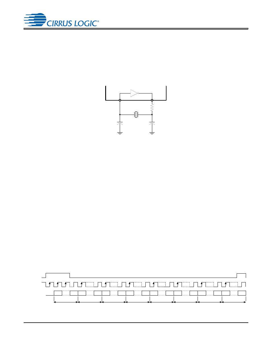
Page 21: Al mode crystal, Figure 10, Cs8421

DS641F6
21
CS8421
CS8421
4.3.7
Clocking
In order to ensure proper operation of the CS8421, the clock or crystal attached to XTI must simultaneous-
ly satisfy the requirements of LRCK for both the input and output as follows:
•
If the input is set to master, Fsi
XTI/128 and Fso XTI/130.
•
If the output is set to master, Fso
XTI/128 and Fsi XTI/130.
•
If both input and output are set to slave, XTI
130*[maximum(Fsi,Fso)], XTI/Fsi < 3750, and XTI/Fso <
3750.
4.4
Time Division Multiplexing (TDM) Mode
TDM Mode allows several CS8421 to be serially connected together allowing their corresponding SDOUT
data to be multiplexed onto one line for input into a DSP or other TDM-capable multichannel device.
The CS8421 can operate in two TDM modes. The first mode consists of all of the CS8421’s output ports set
to slave, as shown in
. The second mode consists of one CS8421 output port set to master and
the remaining CS8421’s output ports set to slave, as shown in
The TDM_IN pin is used to input the data, while the SDOUT pin is used to output the data. The first CS8421
in the chain should have its TDM_IN set to GND. Data is transmitted from SDOUT most significant bit first
on the first OSCLK falling edge after an OLRCK transition and is valid on the rising edge of OSCLK.
In TDM Slave Mode, the number of channels that can by multiplexed to one serial data line depends on the
output sampling rate. For Slave Mode, OSCLK must operate at N*64*Fso, where N is the number of
CS8421’s connected together. The maximum allowable OSCLK frequency is 24.576 MHz, so for Fso =
48 kHz, N = 8 (16 channels of serial audio data).
In TDM Master Mode, OSCLK operates at 256*Fso, which is equivalent to N = 4, so a maximum of 8 chan-
nels of digital audio can be multiplexed together. Note that for TDM Master Mode, MCLK must be at least
256*Fso, where Fso
96 kHz. OLRCK identifies the start of a new frame. Each time-slot is 32-bits wide,
with the valid data sample left-justified within the time-slot. Valid data lengths are 16-, 20-, 24- or 32-bits.
and
show the interface format for Master and Slave TDM Modes with a 32-bit word-length.
XTI
XTO
C
C
R
Figure 10. Typical Connection Diagram for Crystal Circuit
OLRCK
OSCLK
LSB
MSB
LSB
MSB
LSB
MSB
LSB
MSB
LSB
MSB
LSB
MSB
SDOUT/
TDM_IN
SDOUT 3, ch A
32 clks
32 clks
32 clks
32 clks
32 clks
32 clks
LSB
MSB
LSB
MSB
32 clks
32 clks
SDOUT 3, ch B
SDOUT 2, ch A
SDOUT 2, ch B
SDOUT 1, ch A
SDOUT 1, ch B
SDOUT 4, ch A
SDOUT 4, ch B
Figure 11. TDM Slave Mode Timing Diagram
