7 typical connection diagrams, Figure 8, Cs5566 – Cirrus Logic CS5566 User Manual
Page 18
CS5566
18
DS806PP2
5/4/09
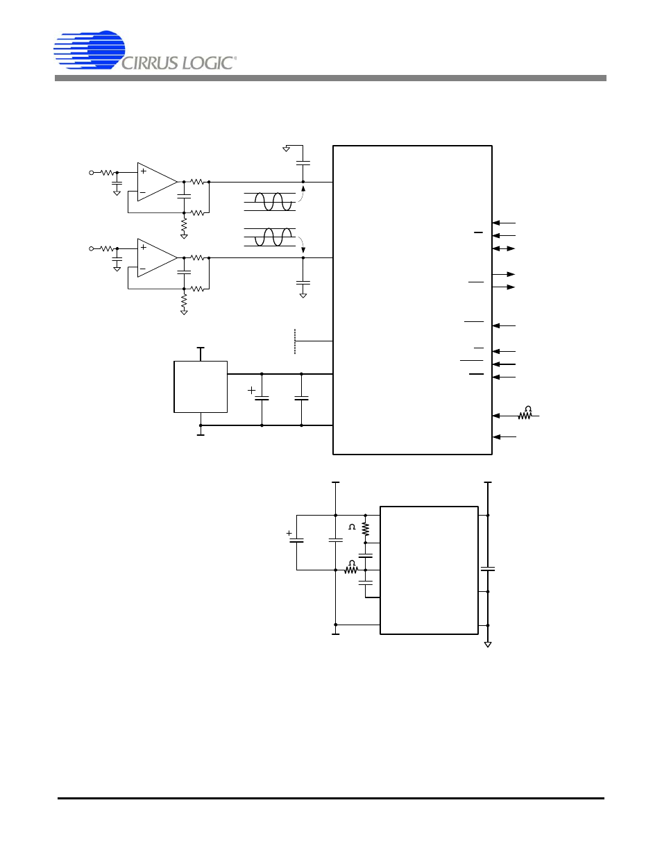
3.7 Typical Connection Diagrams
The following figure depicts the CS5566 powered from bipolar analog supplies, +2.5 V and - 2.5 V.
Figure 8. CS5566 Configured Using
±2.5V Analog Supplies
VREF-
VREF+
+4.096
Voltage
Reference
(NOTE 1)
+2.5 V
SMODE
CS
5
SCLK
5
SDO
RDY
CONV
MCLK
SLEEP
RST
BP/UP
1. See Section 3.3 Voltage Reference for information on required
voltage reference performance criteria.
2.Locate capacitors so as to minimize loop length.
3. The ±2.5 V supplies should also be bypassed to ground at the converter.
4. VLR and the power supply ground for the ±2.5 V should be
connected to the same ground plane under the chip.
5. SCLK and SDO may require pull-down resistors in some applications.
6. An RC input filter can be used to band limit the input to reduce noise.
Select R to be equal to the parallel combination of the feedback of the
feedback resistors 4.99k || 4.99k = 2.5k
0 0
NOTES
-2.5 V
BUFEN
(V-) Buffers Off
(V+) Buffers On
10 µF
0.1 µF
V1+
V2+
V1-
V2-
VL
VLR
DCR
+2.5 V
+3.3 V to +1.8 V
0.1 µF
0.1 µF
X7R
0.1 µF
10
-2.5 V
CS5566
TST
10
0.1 µF
AIN-
AIN+
49.9
47pF
4.99k
4700pF
C0G
49.9
47pF
4.99k
4700pF
C0G
4.99k
4.99k
-2.048 V
+2.048 V
0 V
+2.048 V
-2.048 V
0 V
R
1
R
1
C
1
C
1
50
VLR2
47 µF