Digital characteristics, Digital filter characteristics, Cs5566 – Cirrus Logic CS5566 User Manual
Page 10
CS5566
10
DS806PP2
5/4/09
DIGITAL CHARACTERISTICS
T
A = TMIN to TMAX; VL = 3.3V, ±5% or VL = 2.5V, ±5% or 1.8V, ±5%; VLR = 0V
DIGITAL FILTER CHARACTERISTICS
T
A = TMIN to TMAX; VL = 3.3V, ±5% or VL = 2.5V, ±5% or 1.8V, ±5%; VLR = 0V
16.
See
to understand conversion timing. The 160 MCLK group delay occurs during the 354 MCLK high-power period of a
conversion cycle. See
for more detail.
Parameter
Symbol Min Typ
Max
Unit
Input Leakage Current
I
in
-
-
2
µA
Digital Input Pin Capacitance
C
in
-
3
-
pF
Digital Output Pin Capacitance
C
out
-
3
-
pF
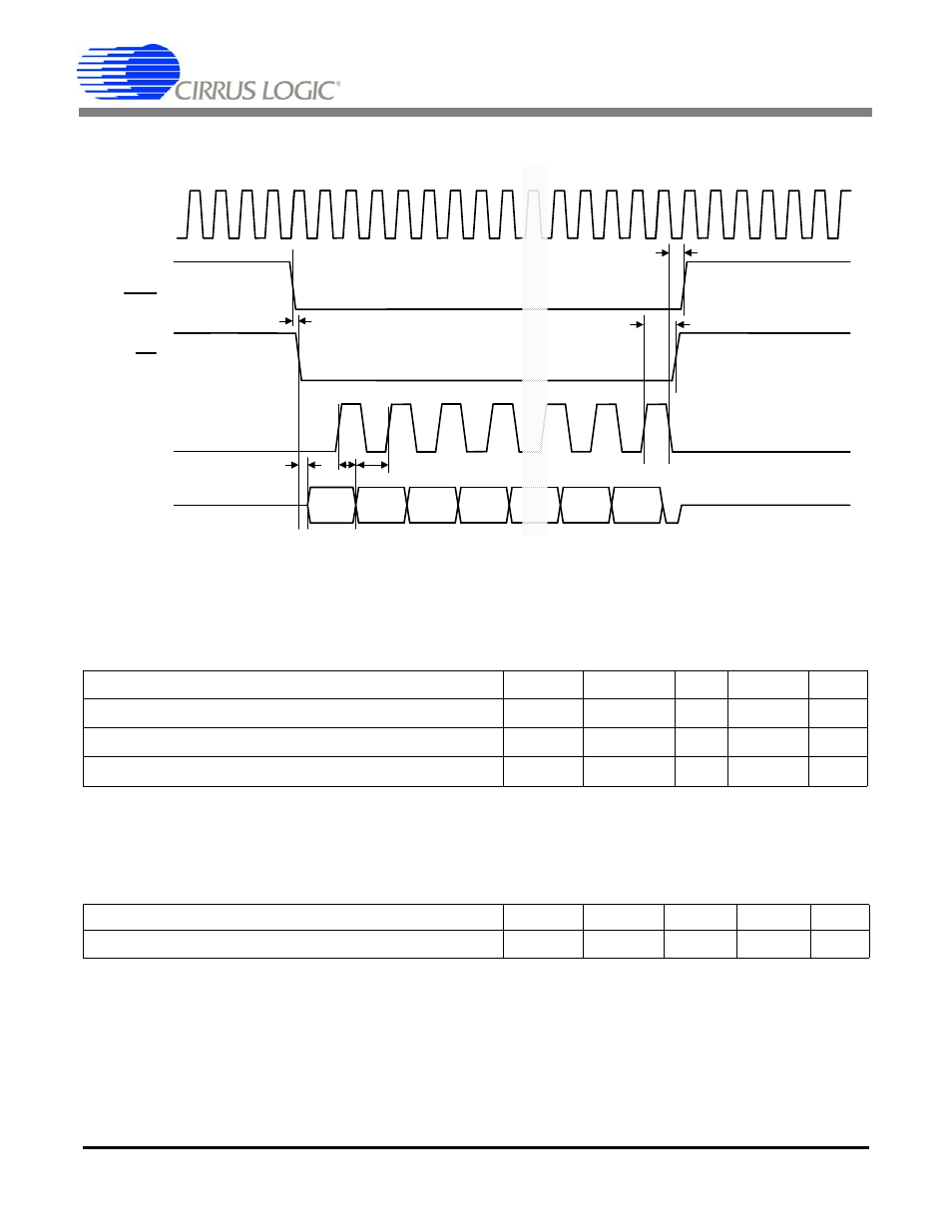
MCLK
SCLK(i)
SDO
CS
RDY
LSB
MSB
t
19
t
18
t
20
t
17
t
15
t
21
Figure 5. SEC Mode - Discontinuous SCLK Read Timing (Not to Scale)
Parameter
Symbol Min Typ
Max
Unit
Group Delay
(Note 16)
-
-
160
-
MCLKs
See also other documents in the category Cirrus Logic Hardware:
- CobraNet (147 pages)
- CS4961xx (54 pages)
- CS150x (8 pages)
- CS1501 (16 pages)
- CS1601 (2 pages)
- CS1601 (16 pages)
- CS1610 (16 pages)
- CRD1610-8W (24 pages)
- CRD1611-8W (25 pages)
- CDB1610-8W (21 pages)
- CS1610A (18 pages)
- CDB1611-8W (21 pages)
- CDB1610A-8W (21 pages)
- CDB1611A-8W (21 pages)
- CRD1610A-8W (24 pages)
- CRD1611A-8W (25 pages)
- CS1615 (16 pages)
- AN403 (15 pages)
- AN401 (14 pages)
- AN400 (15 pages)
- AN375 (27 pages)
- AN376 (9 pages)
- CRD1615-8W (22 pages)
- CRD1616-8W (23 pages)
- AN402 (14 pages)
- AN404 (15 pages)
- CRD1615A-8W (21 pages)
- CS1615A (16 pages)
- CS1630 (56 pages)
- AN374 (35 pages)
- AN368 (80 pages)
- CRD1630-10W (24 pages)
- CRD1631-10W (25 pages)
- CS1680 (16 pages)
- AN405 (13 pages)
- AN379 (31 pages)
- CRD1680-7W (31 pages)
- AN335 (10 pages)
- AN334 (6 pages)
- AN312 (14 pages)
- AN Integrating CobraNet into Audio Products (16 pages)
- CobraNet Audio Routing Primer (9 pages)
- Bundle Assignments in CobraNet Systems (3 pages)
- CS2300-01 (3 pages)
- CS2000-CP (38 pages)