Pin descriptions – Cirrus Logic CS5528 User Manual
Page 49
CS5521/22/23/24/28
DS317F8
49
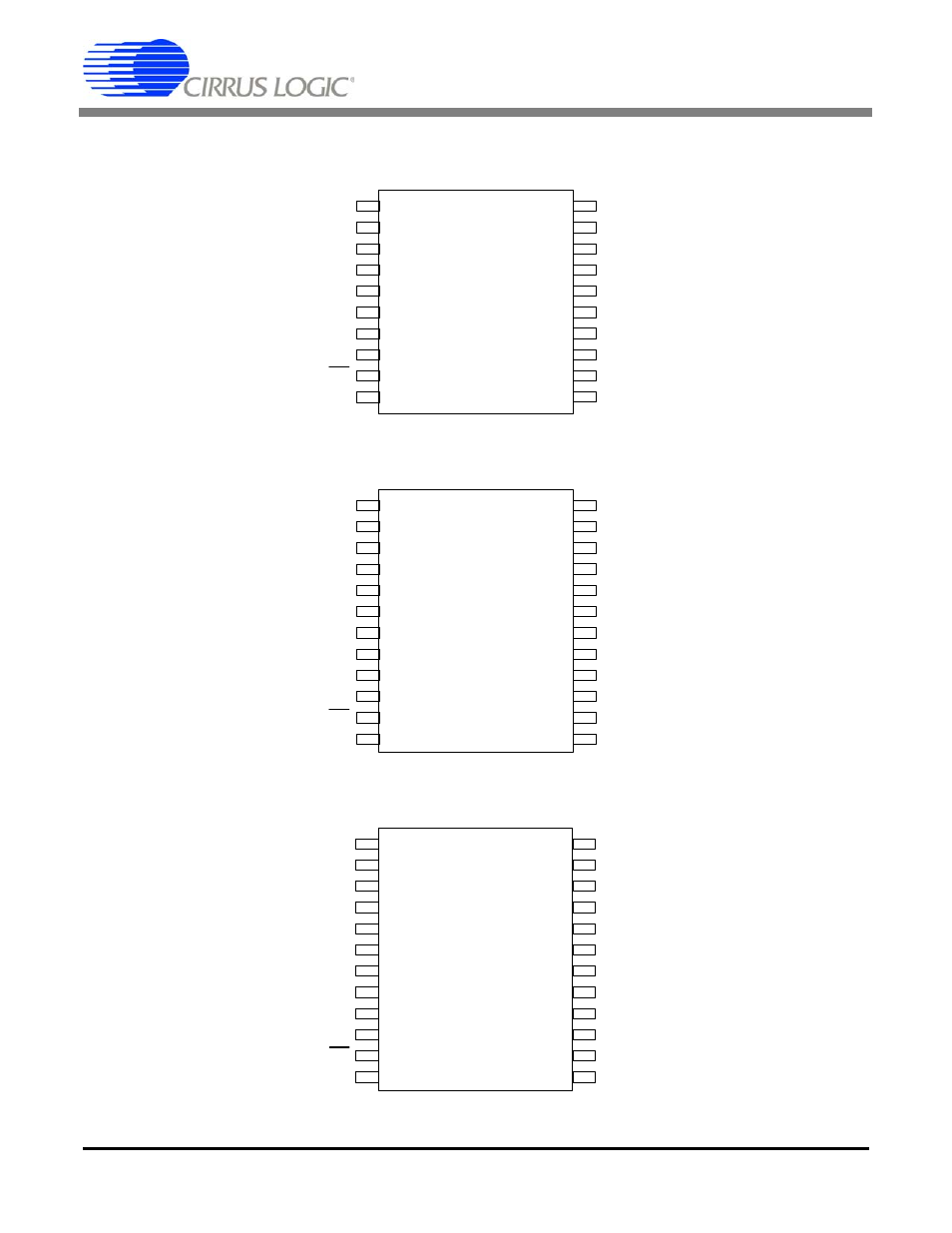
2. PIN DESCRIPTIONS
1
2
3
4
5
6
7
8
13
14
15
16
17
18
19
20
9
11
12
10
CS5521
CS5522
VREF+ Voltage Reference Input
AGND
Analog Ground
VREF-
Voltage Reference Input
VA+
Positive Analog Supply
AIN2+
Differential Analog Input
AIN1+
Differential Analog Input
AIN2-
Differential Analog Input
AIN1-
Differential Analog Input
A1
Logic Output
NBV
Negative Bias Voltage
SCLK
Serial Clock Input
A0
Logic Output
VD+
Positive Digital Supply
CPD
Charge Pump Drive
DGND
Digital Ground
SDI
Serial Data Input
SDO
Serial Data Output
CS
Chip Select
XOUT
Crystal Out
XIN
Crystal In
1
2
3
4
5
6
7
8
17
18
19
20
21
22
23
24
9
13
14
15
16
12
11
10
CS5523
CS5524
VREF+ Voltage Reference Input
AGND
Analog Ground
VREF-
Voltage Reference Input
VA+
Positive Analog Supply
AIN2+
Differential Analog Input
AIN1+
Differential Analog Input
AIN2-
Differential Analog Input
AIN1-
Differential Analog Input
AIN4+
Differential Analog Input
AIN3+
Differential Analog Input
AIN4-
Differential Analog Input
AIN3-
Differential Analog Input
A1
Logic Output
NBV
Negative Bias Voltage
SCLK
Serial Clock Input
A0
Logic Output
VD+
Positive Digital Supply
CPD
Charge Pump Drive
DGND
Digital Ground
SDI
Serial Data Input
SDO
Serial Data Output
CS
Chip Select
XOUT
Crystal Out
XIN
Crystal In
1
2
3
4
5
6
7
8
17
18
19
20
21
22
23
24
9
13
14
15
16
12
11
10
CS5528
VREF+ Voltage Reference Input
AGND
Analog Ground
VREF-
Voltage Reference Input
VA+
Positive Analog Supply
AIN3+
Single-ended Analog Input
AIN1+
Single-ended Analog Input
AIN4+
Single-ended Analog Input
AIN2+
Single-ended Analog Input
AIN7+
Single-ended Analog Input
AIN5+
Single-ended Analog Input
AIN8+
Single-ended Analog Input
AIN6+
Single-ended Analog Input
A1
Logic Output
NBV
Negative Bias Voltage
SCLK
Serial Clock Input
A0
Logic Output
VD+
Positive Digital Supply
CPD
Charge Pump Drive
DGND
Digital Ground
SDI
Serial Data Input
SDO
Serial Data Output
CS
Chip Select
XOUT
Crystal Out
XIN
Crystal In