3 calibration, 1 self calibration, Table 5. offset and gain registers – Cirrus Logic CS5528 User Manual
Page 31: Offset register, Gain register, Corresponds to bit msb-1, n=22). refer to table 5
CS5521/22/23/24/28
DS317F8
31
1.3 Calibration
The CS5521/22/23/24/28 offer four different cali-
bration functions including self calibration and sys-
tem calibration. However, after the devices are
reset, the converter is functional and can perform
measurements without being calibrated. In this
case, the converter will utilize the initialized values
of the on-chip registers (Gain = 1.0, Offset = 0.0)
to calculate output words for the
±100 mV range.
Any initial offset and gain errors in the internal cir-
cuitry of the chip will remain.
The gain and offset registers, which are used for
both self and system calibration, are used to set the
zero and full-scale points of the converter’s transfer
function. One LSB in the offset register is 2
-24
pro-
portion of the input span when the gain register is
set to 1.0 decimal (bipolar span is 2 times the uni-
polar span). The MSB in the offset register deter-
mines if the offset to be trimmed is positive or
negative (0 positive, 1 negative). The converter can
typically trim ±50 percent of the input span. The
gain register spans from 0 to (4 - 2
-22
). The decimal
equivalent meaning of the gain register is:
where the binary numbers have a value of either
zero or one (b
0
corresponds to bit MSB-1, N=22).
Refer to Table 5
for details.
The offset and gain calibration steps each take one
conversion cycle to complete. At the end of the cal-
ibration step, SDO falls to indicate that the calibra-
tion has finished.
1.3.1 Self Calibration
The CS5521/22/23/24/28 offer both self-offset and
self-gain calibrations. For self calibration of offset
in the 25 mV, 55 mV, and 100 mv ranges, the con-
verters internally tie the inputs of the instrumenta-
tion amplifier together and route them to the AIN-
pin as shown in Figure 11 (in the CS5528 they are
routed to AGND). For proper self-calibration of
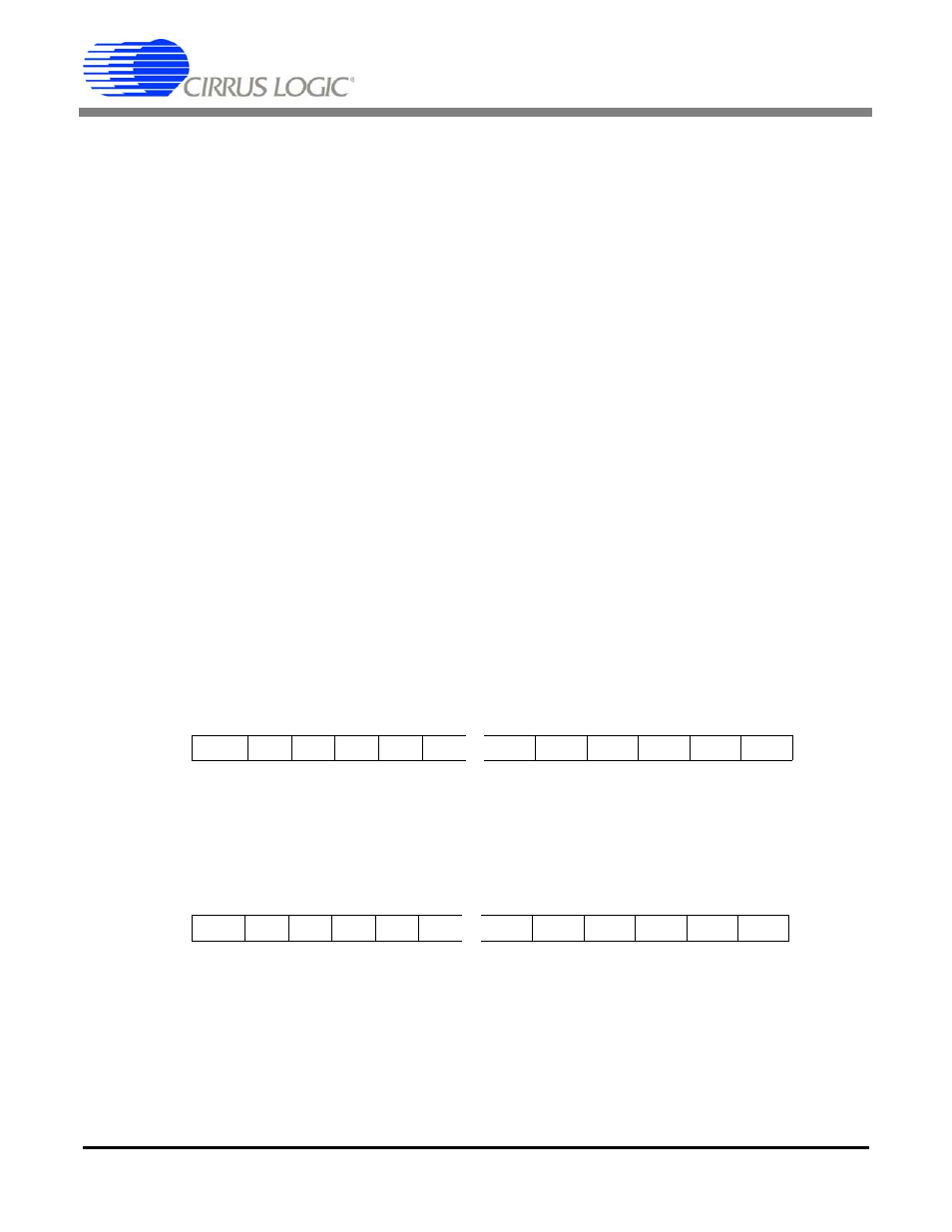
Table 5. Offset and Gain Registers
Offset Register
One LSB represents 2
-24
proportion of the input span when gain register is set to 1.0 decimal (bipolar span is
2 times unipolar span)
Offset and data word bits align by MSB (bit MSB-4 of offset register changes bit MSB-4 of data)
Gain Register
The gain register span is from 0 to (4-2
-22
). After Reset the (MSB-1) bit is 1, all other bits are 0.
MSB
LSB
Register
Sign
2
-2
2
-3
2
-4
2
-5
2
-6
2
-19
2
-20
2
-21
2
-22
2
-23
2
-24
Reset (R)
0
0
0
0
0
0
0
0
0
0
0
0
MSB
LSB
Register
2
1
2
0
2
-1
2
-2
2
-3
2
-4
2
-17
2
-18
2
-19
2
-20
2
-21
2
-22
Reset (R)
0
1
0
0
0
0
0
0
0
0
0
0
≈
≈
D
b
MSB
2
1
b
(
0
2
0
b
1
2
1
–
… b
N
2
N
– )
+
+
+
+
b
MSB
2
1
b
i
2
i
–
i
0
=
N
+
=
=