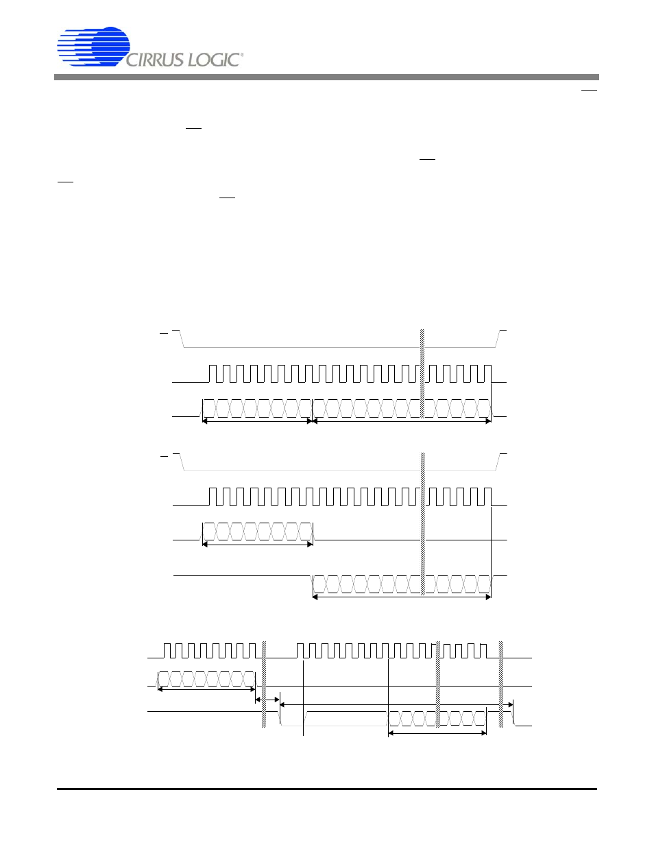
4 serial port interface, Figure 10. command and data word timing – Cirrus Logic CS5528 User Manual
Page 25
CS5521/22/23/24/28
DS317F8
25
1.2.4 Serial Port Interface
The CS5521/22/23/24/28’s serial interface consists
of four control lines: CS, SCLK, SDI, SDO.
Figure 10 illustrates the serial sequence necessary
to write to, or read from the serial port’s registers.
CS (Chip Select) is the control line which enables
access to the serial port. If the CS pin is tied low,
the port can function as a three-wire interface.
SDI (Serial Data In) is the data signal used to trans-
fer data to the converters.
SDO (Serial Data Out) is the data signal used to
transfer output data from the converters. The SDO
output will be held at high impedance any time CS
is at logic 1.
SCLK (Serial Clock) is the serial bit clock which
controls the shifting of data to or from the ADC’s
serial port. The CS pin must be held low (logic 0)
before SCLK transitions can be recognized by the
port logic. To accommodate opto-isolators SCLK
is designed with a Schmitt-trigger input to allow an
opto-isolator with slower rise and fall times to di-
rectly drive the pin. Additionally, SDO is capable
of sinking or sourcing up to 5 mA to directly drive
an opto-isolator LED. SDO will have less than a
400 mV loss in the drive voltage when sinking or
sourcing 5 mA.
Command Time
8 SCLKs
Data Time 24 SCLKs
Write Cycle
CS
SCLK
SDI
MSB
LSB
Command Time
8 SCLKs
CS
SCLK
SDI
Data Time 24 SCLKs
SDO
MSB
LSB
Read Cycle
Command Time
8 SCLKs
8 SCLKs Clear SDO Flag
SDO
SCLK
SDI
Data Time
24 SCLKs
MSB
LSB
* td = XIN/OWR clock cycles for each conversion except the
first conversion which will take XIN/OWR + 7 clock cycles
XIN/OWR
Clock Cycles
t *
d
Figure 10. Command and Data Word Timing