1 instrumentation amplifier, 2 coarse/fine charge buffers, Figure 5. input models for ain+ and ain- pins – Cirrus Logic CS5528 User Manual
Page 14
CS5521/22/23/24/28
14
DS317F8
1.1.1 Instrumentation Amplifier
The instrumentation amplifier is chopper stabilized
and is activated any time conversions are performed
with the low-level input ranges,
≤100 mV. The am-
plifier is powered from VA+ and from the NBV
(Negative Bias Voltage) pin allowing the
CS5521/22/23/24/28 to be operated in either of two
analog input configurations. The NBV pin can be bi-
ased to a negative voltage between -1.8 V and
-2.5 V, or tied to AGND (for the CS5528, NBV has
to be between -1.8 V and -2.5 V for the ranges below
100 mV when the amplifier is engaged). The com-
mon-mode-plus-signal range of the instrumentation
amplifier is 1.85 V to 2.65 V with NBV grounded.
The common-mode-plus-signal range of the instru-
mentation amplifier is -0.150 V to 0.950 V with
NBV between -1.8 V to -2.5 V. Whether NBV is
tied between -1.8 V and -2.5 V or tied to AGND,
the (Common Mode + Signal) input on AIN+ and
AIN- must stay between NBV and VA+.
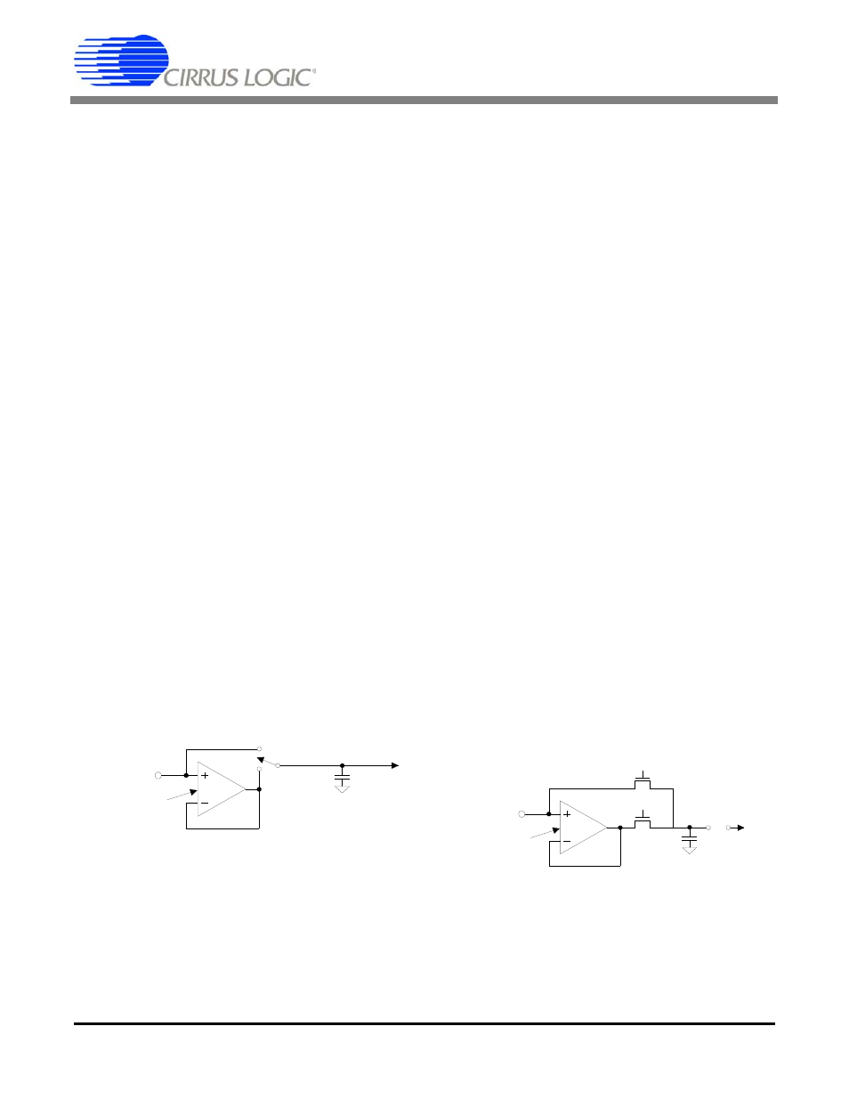
Figure 5
illustrates an analog input model for the
ADCs when the instrumentation amplifier is en-
gaged. The CVF (sampling) input current for each
of the analog input pins depends on the CFS1 and
CFS0 (Chop Frequency Select) bits in the configu-
ration register (see Configuration Register for de-
tails). Note that the CVF current is lowest with the
CFS bits in their default states (cleared to logic 0s).
Further note that the CVF current into the instru-
mentation amplifier is less than 300 pA over -40°C
to +85°C. Note that Figure 5 is for input current
modeling only. For physical input capacitance see
‘Input Capacitance’ specification under ANALOG
CHARACTERISTICS. Also refer to Applications
and input sampling currents.
Note: Residual noise appears in the converter’s baseband for
output word rates greater than 61.6 Sps if the CFS bits
are logic 0 (chop clock = 256 Hz). For word rates of
30 Sps and lower, 256 Sps chopping is recommended,
and for 61.6 Sps, 84.5 Sps and 101.1 Sps word rate set-
tings, 4096 Hz chopping is recommended.
1.1.2 Coarse/Fine Charge Buffers
The unity gain buffers are activated any time conver-
sions are performed with the high-level inputs rang-
es, 1 V, 2.5 V, and 5 V. The unity gain buffers are
designed to accommodate rail-to-rail input signals.
The common-mode-plus-signal range for the unity
gain buffer amplifier is NBV to VA+.
Typical CVF (sampling) current for the unity gain
buffer amplifiers is about 10 nA
(XIN = 32.768 kHz, see Figure 6).
A IN
2 5 m V , 5 5 m V , a nd 10 0 m V R a n g e s
C = 48 p F
C F S 1 /C F S 0 = 00 , f = 2 5 6 H z
C F S 1 /C F S 0 = 01 , f = 4 0 9 6 H z
C F S 1 /C F S 0 = 10 , f = 1 6 .38 4 k H z
C F S 1 /C F S 0 = 11 , f = 1 0 2 4 H z
V
≤ 25 m V
i = fV
C
o s
os
n
Figure 5. Input Models for AIN+ and AIN- pins,
≤
100
mV Input Ranges
A IN
C = 2 0 p F
f = 3 2 .7 6 8 kH z
φ C oarse
1
φ Fine
1
V
≤ 25 m V
i = fV
C
o s
o s
n
1 V , 2 .5 V a n d 5 V R a n g e s
Figure 6. Input Models for AIN+ and AIN- pins,
>
100
mV input ranges
,