Cirrus Logic CS5528 User Manual
Features, General description, Scalable input span (bipolar/unipolar)
Copyright
Cirrus Logic, Inc. 2009
(All Rights Reserved)
CS5521/22/23/24/28
16-bit or 24-bit, 2/4/8-channel ADCs with PGIA
Features
Low Input Current (100 pA), Chopper-
stabilized Instrumentation Amplifier
Scalable Input Span (Bipolar/Unipolar)
- 2.5V VREF: 25 mV, 55 mV, 100 mV, 1 V,
2.5 V, 5 V
- External: 10 V, 100 V
Wide V
REF
Input Range (+1 to +5 V)
Fourth Order Delta-Sigma A/D Converter
Easy to Use Three-wire Serial Interface Port
- Programmable/Auto Channel Sequencer with
Conversion Data FIFO
- Accessible Calibration Registers per Channel
- Compatible with SPI™
and Microwire™
System and Self Calibration
Eight Selectable Word Rates
- Up to 617 Sps (XIN = 200 kHz)
- Single Conversion Settling
- 50/60 Hz ±3 Hz Simultaneous Rejection
Single +5 V Power Supply Operation
- Charge Pump Drive for Negative Supply
- +3 to +5 V Digital Supply Operation
Low Power Consumption: 6.0 mW
General Description
The CS5521/22/23/24/28 are highly integrated
ΔΣ ana-
log-to-digital converters (ADCs) which use charge-
balance techniques to achieve 16-bit (CS5521/23) and
24-bit (CS5522/24/28) performance. The ADCs come as
either two-channel (CS5521/22), four-channel
(CS5523/24), or eight-channel (CS5528) devices and
include a low-input-current, chopper-stabilized instru-
mentation amplifier. To permit selectable input spans of
25 mV, 55 mV, 100 mV, 1 V, 2.5 V, and 5 V, the ADCs
include a PGA (programmable gain amplifier). To ac-
commodate ground-based thermocouple applications,
the devices include a charge pump drive which provides
a negative bias voltage to the on-chip amplifiers.
These devices also include a fourth-order
ΔΣ modulator
followed by a digital filter which provides eight selectable
output word rates. The digital filters are designed to settle
to full accuracy within one conversion cycle and when
operated at word rates below 30 Sps, they reject both
50 Hz and 60 Hz interference.
These single-supply products are ideal solutions for
measuring isolated and non-isolated, low-level signals in
process control applications.
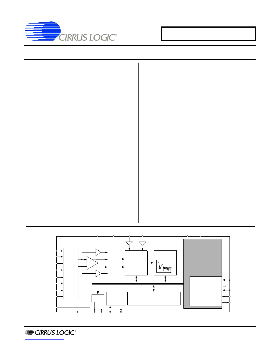
ORDERING INFORMATION
VA+
AGND
VREF+ VREF-
VD+
DGND
XIN XOUT
NBV
Latch
Differential
Digital Filter
4
th
Order
ΔΣ
Modulator
Clock
Gen.
MUX
AIN2+
X1
X1
X1
CS5524
Shown
AIN2-
AIN1+
AIN1-
AIN4+
AIN4-
AIN3+
AIN3-
A0 A1
CPD
Controller,
Pr
og
ra
mma
b
le
Gai
n
Setup Registers,
&
Data FIFO &
Calibration Registers
Channel Scan
Logic
Serial Port
Interface
+
X20
SDO
SDI
SCLK
CS
JUL ‘09
DS317F8
Document Outline
- Features
- Table of Contents
- List of Figures
- List of Tables
- Characteristics & Specifications
- ANALOG CHARACTERISTICS
- Typical RMS Noise, CS5521/23
- Typical Noise Free Resolution (Bits), CS5521/23
- Typical RMS Noise, CS5522/24/28
- Typical Noise Free Resolution (Bits), CS5522/24/28
- 5 v DIGITAL CHARACTERISTICS
- 3 v DIGITAL CHARACTERISTICS
- DYNAMIC CHARACTERISTICS
- RECOMMENDED OPERATING CONDITIONS
- ABSOLUTE MAXIMUM RATINGS
- SWITCHING CHARACTERISTICS
- 1. General Description
- 1.1 Analog Input
- 1.2 Overview of ADC Register Structure and Operating Modes
- 1.3 Calibration
- 1.4 Performing Conversions and Reading the Data Conversion FIFO
- 1.5 Conversion Output Coding
- 1.6 Digital Filter
- 1.7 Clock Generator
- 1.8 Power Supply Arrangements
- 1.9 Digital Gain Scaling
- 1.10 Getting Started
- 1.11 PCB Layout
- 2. PIN DESCRIPTIONS
- 3. SPECIFICATION DEFINITIONS
- 4. ORDERING Information
- 5. Environmental, Manufacturing, & Handling Information
- 6. Package Dimension Drawings