5 voltage reference, Voltage reference, Figure 7. input ranges greater than 5 v – Cirrus Logic CS5528 User Manual
Page 16: Figure 8. input model for vref+ and vref- pins
CS5521/22/23/24/28
16
DS317F8
mentation amplifier with a gain range setting of
100 mV or less, is typically 100 pA. This is low
enough to permit large external resistors to divide
down a large external signal without significant
fer to
Application Note 158
for more details on
high-voltage (>5 V) measurement.
1.1.5 Voltage Reference
The CS5521/22/23/24/28 devices are specified for
operation with a 2.5 V reference voltage between
the VREF+ and VREF- pins of the device. For a
single-ended reference voltage, such as the
LT1019-2.5, the reference voltage is input into the
VREF+ pin of the converter and the VREF- pin is
grounded.
The differential voltage between the VREF+ and
VREF- can be any voltage from 1.0 V up to VA+,
however, the VREF+ cannot go above VA+ and the
VREF- pin can not go below NBV.
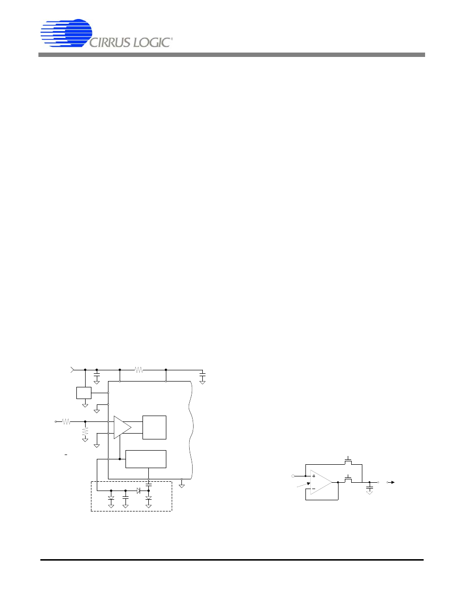
Figure 8 illustrates the input models for the VREF
pins. The dynamic input current for each of the pins
can be determined from the models shown.
1.2 Overview of ADC Register Structure
and Operating Modes
The CS5521/22/23/24/28 ADCs have an on-chip
controller, which includes a number of user-acces-
sible registers. The registers are used to hold offset
and gain calibration results, configure the chip's
operating modes, hold conversion instructions, and
to store conversion data words. Figure 9 depicts a
block diagram of the on-chip controller’s internal
registers for the CS5523/24.
Each of the converters has 24-bit registers to func-
tion as offset and gain calibration registers for each
channel. The converters with two channels have
two offset and two gain calibration registers, the
converters with four channels have four offset and
four gain calibration registers, and the eight chan-
nel converter has eight offset and eight gain cali-
bration registers. These registers hold calibration
results. The contents of these registers can be read
or written by the user. This allows calibration data
to be off-loaded into an external EEPROM. The
user can also manipulate the contents of these reg-
isters to modify the offset or the gain slope of the
converter.
The converters include a 24-bit configuration reg-
ister of which 17 of the bits are used for setting op-
tions such as the conversion mode, operating power
options, setting the chop clock rate of the instru-
Voltage
Divider
PGIA set for
+ 100 mV
±10V
Charge Pump
Regulator
ΔΣ ADC
PGIA
+5 V
2.5 V
VA+
VREF+
VREF-
VD+
+
-
NBV
V
≈ -2.1 V
+
10
μF
0.033
μF
CPD
0.1
μF
10
Ω
0.1
μF
1N4148
1N4148
BAT85
Charge Pump
Circuitry
DGND
chop clock = 256 Hz
10 K
Ω
1 M
Ω
Figure 7. Input Ranges Greater than 5 V
V R E F
C = 1 0 p F
f = 3 2 .7 6 8 k H z
2
φ Fine
1
V
≤ 25m V
i = fV C
os
os
n
φ C oarse
Figure 8. Input Model for VREF+ and VREF- Pins