1 charge pump drive circuits, 9 digital gain scaling, F ceramic ca- pacitors in parallel can be used – Cirrus Logic CS5528 User Manual
Page 45
CS5521/22/23/24/28
DS317F8
45
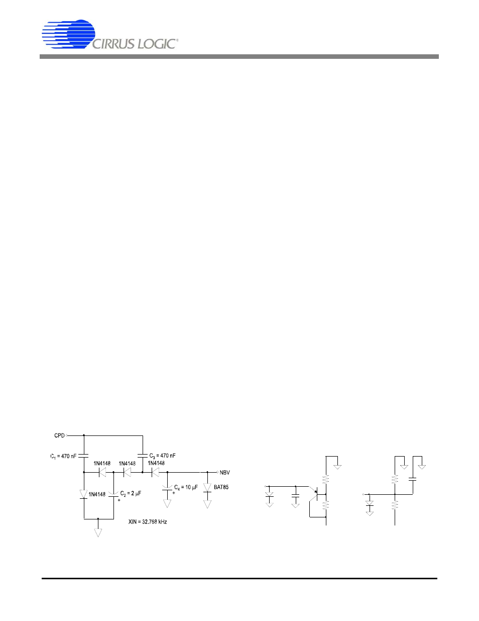
1.8.1 Charge Pump Drive Circuits
The CPD (Charge Pump Drive) pin of the converter
can be used with external components (shown in
Figure 21) to develop an appropriate negative bias
voltage for the NBV pin. When CPD is used to gen-
erate the NBV, the NBV voltage is regulated with
an internal regulator loop referenced to VA+.
Therefore, any change on VA+ results in a propor-
tional change on NBV. With VA+ = 5 V, NBV’s
regulation is set proportional to VA+ at approxi-
mately -2.1 V.
Figure 24 illustrates a charge pump circuit when
the converters are powered from a +3.0 V digital
supply. Alternatively, the negative bias supply can
be generated from a negative supply voltage or a
resistive divider as illustrated in Figure 25.
For ground-based signals with the instrumentation
amplifier engaged (when in the 25 mV, 55 mV, or
100 mV ranges), the voltage on the NBV pin
should at no time be less negative than -1.8 V or
more negative than -2.5 V. To prevent excessive
voltage stress to the chip when the instrumentation
amplifier isn’t engaged (when in the 1 V, 2.5 V, or
5 V ranges) the NBV voltage should not be more
negative than -2.5 V.
The components in Figure 21 are the preferred
components for the CPD filter. However, smaller
capacitors can be used with acceptable results. The
10
μ
F ensures very low ripple on NBV. Intrinsic
safety requirements prohibit the use of electrolytic
capacitors. In this case, four 0.47
μ
F ceramic ca-
pacitors in parallel can be used.
Note: The charge pump is designed to nominally provide
400
μ
A of current for the instrumentation amplifier
when a 0.033
μ
F pumping capacitor is used
(XIN = 32.768 kHz). When a larger pumping capaci-
tor is used, the charge pump can source more current
to power external loads. Refer to Applications Note
152 “Using the CS5521/23, CS5522/24/28, and
CS5525/26 Charge Pump Drive for External Loads”
for more details on using the charge pump with exter-
nal loads.
1.9 Digital Gain Scaling
The CS5521/22/23/24 and CS5528 all feature a
gain register capable of being scaled from 0.6 to 4-
2
-22
in decimal. The specified ranges of the con-
verter are defined with a voltage reference of 2.5 V
and the gain register set at approximately 1.0. The
gain register can be manipulated to scale the input
for ranges other than those specified. For example,
when using a 2.5 V voltage reference, and the
25 mV input range setting, the gain register can be
changed from 1.000 to 2.000 (shift the entire regis-
ter contents to the left one position) to achieve an
input span of 12.5 mV. Under this condition the
full span of the converter codes will appear across
a 12.5 mV span. The amount of noise in the con-
Figure 24. Charge Pump Drive Circuit for VD+ = 3 V
-5 V
N B V
3 0 .1 K
Ω
3 4 .8 K
Ω
2 N 5 0 8 7
o r s im ila r
-5V
2 .1 K
Ω
2 .0 K
Ω
N B V
+
1 0
μF
1 0
μF
+
BAT85
BAT85
Figure 25. Alternate NBV Circuits