3 analog section, Cdb5460au – Cirrus Logic CDB5460AU User Manual
Page 4
CDB5460AU
4
DS487DBU1
1.3
Analog Section
The CDB5460AU evaluation board provides screw-type terminals (J23, J27) to connect input signals to the voltage
and current channels. The screw terminals are labels as VIN+, VIN-, IIN+, and IIN-. A simple RC network at each
channel input provides a simple anti-alias filter.
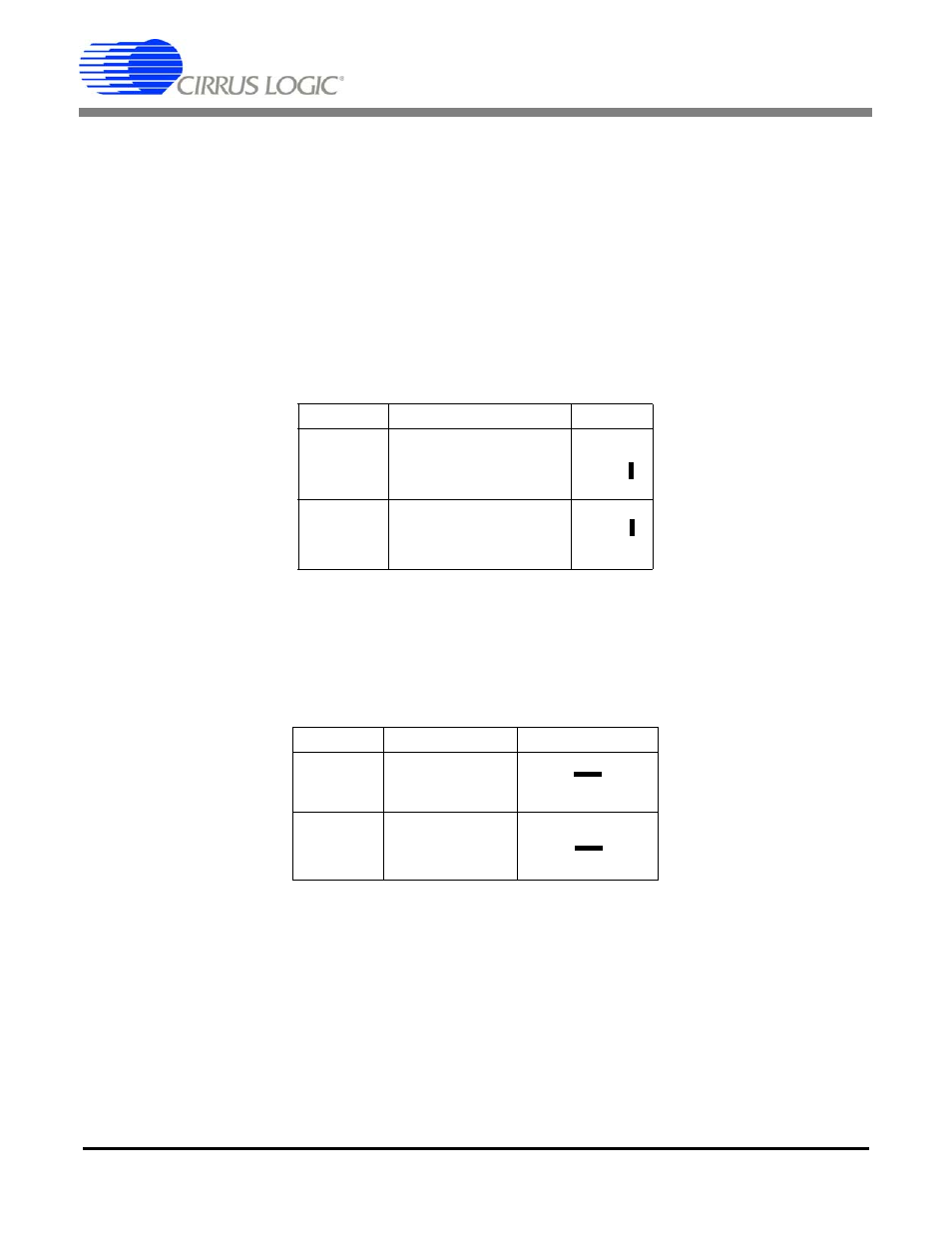
The evaluation board provides three voltage reference options for VREFIN to the CS5460A. The three voltage ref-
erence options include: VREFOUT from the CS5460A, the on-board +2.5V reference, and external REF+ (screw
terminal J14). Table 1 and Table 2 illustrate the options available for VREFIN. With a jumper on J25 in the position
labeled VREFOUT, the reference is supplied by the on-chip voltage reference. With a jumper on J25 in the position
labeled VREF, the reference is supplied by an off-chip voltage reference.
Table 2 illustrates the options available for VREF. With a jumper on J12 in position LT1019, the LT1019 provides a
+2.5V reference (the LT1019 was chosen for its low drift — typically 20ppm/°C). By setting the jumper on J12 to
position REF+, an external voltage reference is supplied via screw terminal J14's REF+ input.
The three input signal options for the voltage (VIN±) and current (IIN±) channel input include: an external signal
(screw terminals J23 and J27), GND, or VREF. Table3 illustrates the options available. By installing jumpers on J17
to position VIN+, J22 to position VIN-, J24 to position IIN+, and J26 to position IIN-, the input voltage signal is sup-
plied from the screw terminals J23 and J27. With a jumper on J17, J22, J24, and J26 in the GND position, the inputs
Reference
Description
J25
VREFOUT
Selects On-chip
Reference (30 ppm/
°
C)
VREF
Selects External or
LT1019 Reference(J12)
Table 1. Internal Voltage Reference Selection for VREF
Reference
Description
J12
LT1019
Selects On-board
LT1019 Reference
(20 ppm/
°
C)
REF+
Selects External
Reference Source
(J14)
Table 2. External Voltage Reference Selection for VREF
O
O
VREF
VREFIN
VREFOUT
(Default)
O
O
VREF
VREFIN
VREFOUT
O
VREF
O O
VREF
LT1019
REF+
O
VREF
O O
VREF
LT1019
REF+
(Default)