Hardware mode control, 1 fpga h/w control, Table 1. mclk and clock/data routing options – Cirrus Logic CDB42L51 User Manual
Page 13: Section 3. “hardware mode control” on, Section 3
DS679DB2
13
CDB42L51
3. HARDWARE MODE CONTROL
The CDB may be configured without the use of a software control port through the use of two switches, “FPGA H/W
Control” and “CS42L51 H/W Control.” These switches are enabled in hardware mode only and ignored in software
mode. The CDB42L51 automatically enters hardware mode upon initial power up, or when exiting software mode,
by terminating the Cirrus FlexGUI software or by disconnecting the RS-232 serial cable.
3.1
FPGA H/W Control
The “FPGA H/W Control” switch sets up the CDB in 11 pre-defined routing topologies in hardware mode.
The tables and figures below describe each switch setting. The At-A-Glance Controls table provides a quick
reference for all presets.
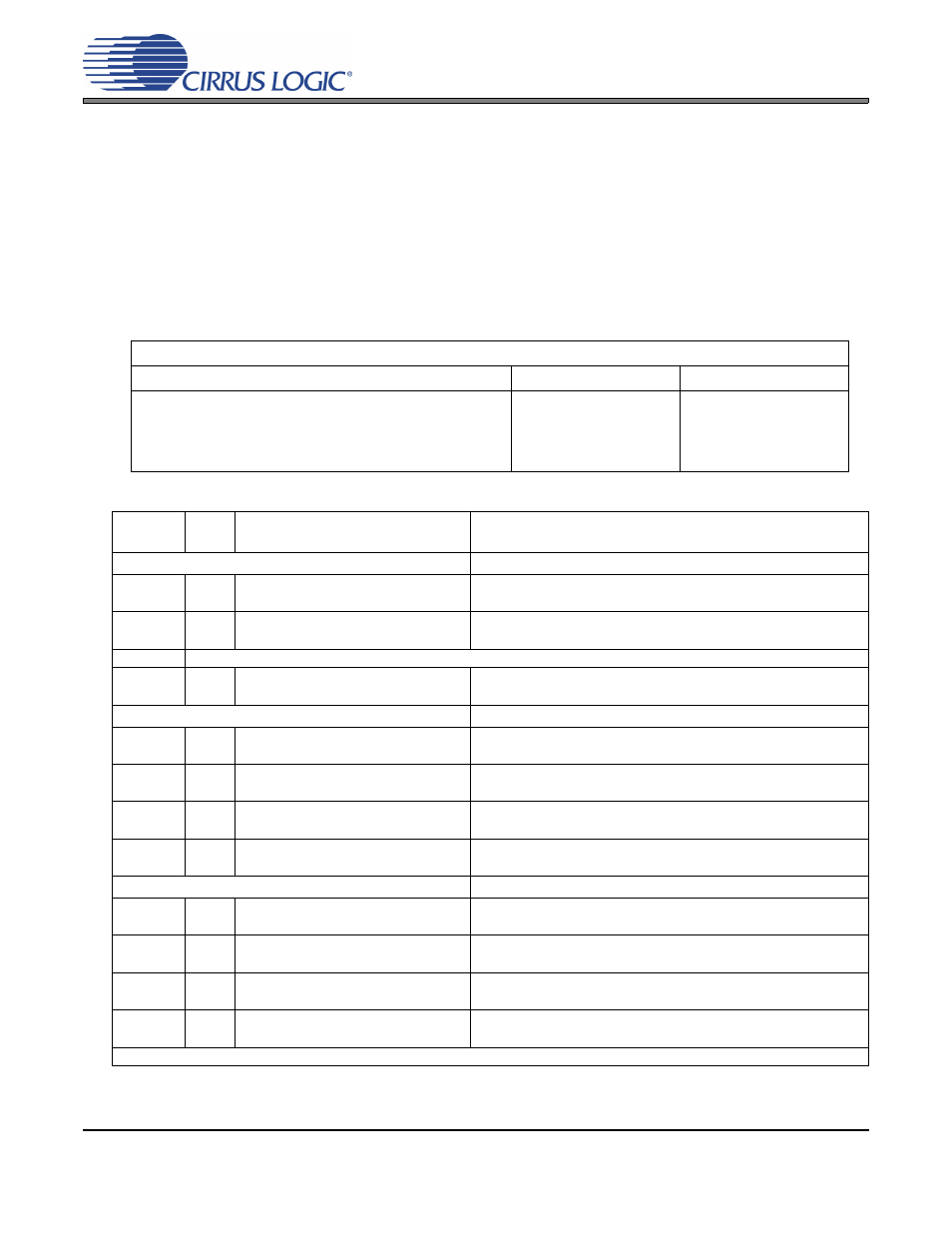
At-A-Glance Controls
S[3:2]
S[1]
S[0]
00 - CS8415 MCLK / CS8415 clocks/data route through FPGA
0 - CS42L51 Slave Routing
1 - CS42L51 Master Routing
0 - No Loopback Routing
1 - Loopback Routing
01 - I/O Header MCLK / I/O Header clocks/data route through FPGA
10 - Oscillator MCLK / I/O Header clocks/data route through FPGA
11 - Reserved
Signal
Routing
S[3:0]
General Description
Detailed Description
CS8415 MCLK
0
0000 CS8415 Clocks/Data
1) CS8415 masters MCLK. 2) CS8415 masters PCM clocks.
3) CS8415 data into SDIN.
1
0001 CS8415 Clocks, ADC Loopback
1) CS8415 masters MCLK. 2) CS8415 masters PCM clocks.
3) SDOUT into SDIN.
2
Reserved
3
0011 CS42L51 Clocks, ADC Loopback
1) CS8415 masters MCLK. 2) CS42L51 masters PCM clocks.
3) SDOUT into SDIN.
I/O MCLK
4
0100 I/O Clocks/Data
1) I/O masters MCLK. 2) I/O masters PCM clocks.
3) I/O data into SDIN.
5
0101 I/O Clocks, ADC Loopback
1) I/O masters MCLK. 2) I/O masters PCM clocks.
3) SDOUT into SDIN.
6
0110 CS42L51 Clocks, I/O Data
1) I/O masters MCLK. 2) CS42L51 masters PCM clocks.
3) I/O data into SDIN.
7
0111 CS42L51 Clocks, ADC Loopback
1) I/O masters MCLK. 2) CS42L51 masters PCM clocks.
3) SDOUT into SDIN.
Oscillator MCLK
8
1000 I/O Clocks/Data
1) Oscillator masters MCLK. 2) I/O masters PCM clocks.
3) I/O data into SDIN.
9
1001 I/O Clocks, ADC Loopback
1) Oscillator masters MCLK. 2) I/O masters PCM clocks.
3) SDOUT into SDIN.
10
1010 CS42L51 Clocks, I/O Data
1) Oscillator masters MCLK. 2) CS42L51 masters PCM clocks.
3) I/O data into SDIN.
11
1011 CS42L51 Clocks, ADC Loopback
1) Oscillator masters MCLK. 2) CS42L51 masters PCM clocks.
3) SDOUT into SDIN.
12-15 Reserved
Table 1. MCLK and Clock/Data Routing Options