8 signal and power-up requirements, 1 power-up requirements, Signal sequence and timing description – AMD SEMPRON 10 User Manual
Page 51: Signal and power-up requirements, Sequence, 8signal and power-up requirements
Chapter 8
Signal and Power-Up Requirements
39
31994A —1 August 2004
AMD Sempron™ Processor Model 10 with 256K L2 Cache Data Sheet
8
Signal and Power-Up Requirements
The AMD Sempron™ processor model 10 is designed to provide
functional operation if the voltage and temperature parameters
are within the limits of normal operating ranges.
8.1
Power-Up Requirements
Signal Sequence and
Timing Description
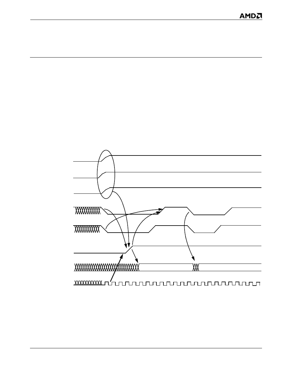
Figure 12 shows the relationship between key signals in the
system during a power-up sequence. This figure details the
requirements of the processor.
Figure 12. Signal Relationship Requirements During Power-Up Sequence
Notes: 1. Figure 12 represents several signals generically by using names not necessarily consistent
with any pin lists or schematics.
2. Requirements 1–8 in Figure 12 are described in “Power-Up Timing Requirements” on page 40.
3.3 V Supply
VCCA (2.5 V)
(for PLL)
RESET#
VCC_CORE
(Processor Core)
NB_RESET#
PWROK
System Clock
2
1
3
4
5
6
FID[3:0]
7
8
Warm reset
condition