AMD SEMPRON 10 User Manual
Page 45
Chapter 7
Electrical Data
33
31994A —1 August 2004
AMD Sempron™ Processor Model 10 with 256K L2 Cache Data Sheet
T
SU
Sync Input Setup Time
2.0
ns
4, 5
T
HD
Sync Input Hold Time
0.0
ps
4, 5
T
DELAY
Output Delay with respect to RSTCLK
0.0
6.1
ns
5
T
BIT
Input Time to Acquire
20.0
ns
7, 8
T
RPT
Input Time to Reacquire
40.0
ns
9–13
T
RISE
Signal Rise Time
1.0
3.0
V/ns
6
T
FALL
Signal Fall Time
1.0
3.0
V/ns
6
C
P
IN
Pin Capacitance
4
12
pF
T
VALID
Time to data valid
100
ns
14
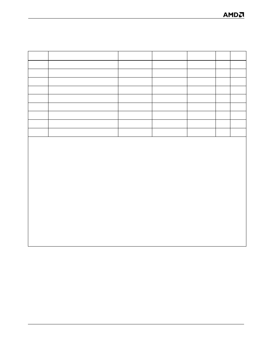
Table 12. General AC and DC Characteristics (continued)
Symbol
Parameter Description
Condition
Min
Max
Units
Notes
Notes:
1. Characterized across DC supply voltage range.
2. Values specified at nominal V
CC_CORE
. Scale parameters between V
CC_CORE.
minimum and V
CC_CORE.
maximum.
3. I
OL
and I
OH
are measured at V
OL
maximum and V
OH
minimum, respectively.
4. Synchronous inputs/outputs are specified with respect to RSTCLK and RSTCK# at the pins.
5. These are aggregate numbers.
6. Edge rates indicate the range over which inputs were characterized.
7. In asynchronous operation, the signal must persist for this time to enable capture.
8. This value assumes RSTCLK period is 10 ns ==> TBIT = 2*fRST.
9. The approximate value for standard case in normal mode operation.
10. This value is dependent on RSTCLK frequency, divisors, Low Power mode, and core frequency.
11. Reassertions of the signal within this time are not guaranteed to be seen by the core.
12. This value assumes that the skew between RSTCLK and K7CLKOUT is much less than one phase.
13. This value assumes RSTCLK and K7CLKOUT are running at the same frequency, though the processor is capable of other
configurations.
14. Time to valid is for any open-drain pins. See requirements 7 and 8 in the “Power-Up Timing Requirements“ chapter for more
information.