3 voltage identification (vid[4:0]), Table 6, Vid[4:0] dc characteristics – AMD SEMPRON 10 User Manual
Page 38
26
Electrical Data
Chapter 7
AMD Sempron™ Processor Model 10 with 256K L2 Cache Data Sheet
31994A —1 August 2004
7.3
Voltage Identification (VID[4:0])
Table 6 shows the VID[4:0] DC Characteristics. For more
information on VID[4:0] DC Characteristics, see “VID[4:0]
Pins” on page 74.
Southbridge
RESET#, INTR, NMI, SMI#, INIT#, A20M#,
FERR, IGNNE#, STPCLK#, FLUSH#
See “General AC and DC Characteristics” on page 32,
“INTR Pin” on page 72, “NMI Pin” on page 72, “SMI#
Pin” on page 73, “INIT# Pin” on page 71, “A20M# Pin”
on page 68, “FERR Pin” on page 69,“IGNNE# Pin” on
page 71, “STPCLK# Pin” on page 73, and “FLUSH# Pin”
on page 71.
JTAG
TMS, TCK, TRST#, TDI, TDO
See “General AC and DC Characteristics” on page 32.
Test
PLLBYPASS#, PLLTEST#, PLLMON1,
PLLMON2, SCANCLK1, SCANCLK2,
SCANSHIFTEN, SCANINTEVAL, ANALOG
See “General AC and DC Characteristics” on page 32,
“PLL Bypass and Test Pins” on page 72, “Scan Pins” on
page 73, “Analog Pin” on page 68.
Miscellaneous DBREQ#, DBRDY, PWROK
See “General AC and DC Characteristics” on page 32,
“DBRDY and DBREQ# Pins” on page 69, “PWROK Pin”
on page 73.
APIC
PICD[1:0]#, PICCLK
See “APIC Pins AC and DC Characteristics” on page 37,
and “APIC Pins, PICCLK, PICD[1:0]#” on page 68.
Thermal
THERMDA, THERMDC
See Table 13, “Thermal Diode Electrical Characteristics,”
on page 35, and “THERMDA and THERMDC Pins” on
page 73.
Table 5.
Interface Signal Groupings (continued)
Signal Group
Signals
Notes
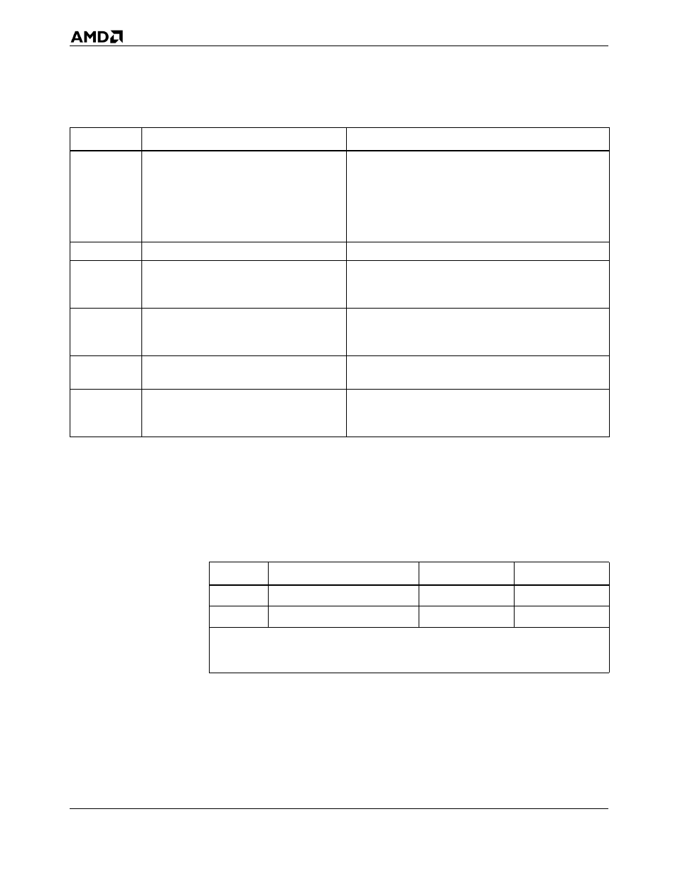
Table 6.
VID[4:0] DC Characteristics
Parameter
Description
Min
Max
I
OL
Output Current Low
6 mA
V
OH
Output High Voltage
–
5.25 V *
Note:
*
The VID pins are either open circuit or pulled to ground. It is recommended that these pins
are not pulled above 5.25 V, which is 5.0 V + 5%.