Dt-5txr with dop-bcd module – SHIMPO DT-5TS User Manual
Page 18
18
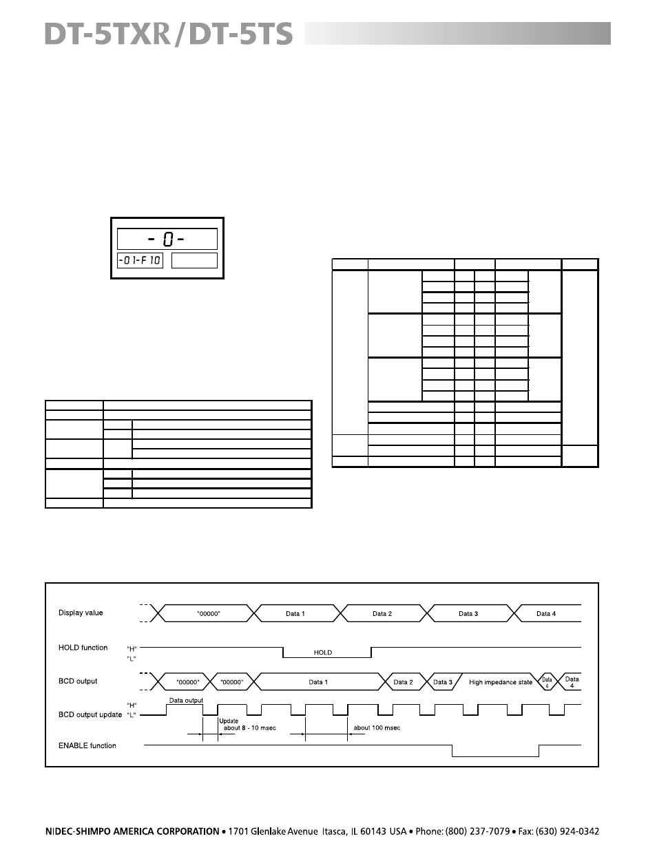
The waveforms below give a synopsis of how the output
BCD data behave during the time the different control
functions become active.
The waveforms show that when the ENABLE function is
LO, the BCD output data goes to a high impedance state
to facilitate the selection of one unique DT-5TXR-BCD unit
among several that might be feeding the same PLC. At
the same time, when the HOLD function goes LO, the
BCD data stop changing, though the display value changes
according to the new information fed into the DT-5TX.
This provides time for the PLC to catch up (if needed).
The BCD data can only change when the update time
signal is low.
The table below shows the pin assignments of the 36-pin
connector relative to the DOP-BCD.
I/O
O
/I
1
1
19
1
2
2
20
2
4
3
21
4
8
4
22
8
1
5
23
1
2
6
24
2
4
7
25
4
8
8
26
8
1
9
27
1
2
10
28
2
4
11
29
4
8
12
30
8
13
31
14
32
15
33
16
34
17
35
18
36
Input
Output
DESIGNATION
PIN No.
DESIGNATION
PLUS
X 10
3
X 10
4
X 10
5
DP 1
Output
X 10
2
X 10
1
X 10
0
GND
ENABLE
HOLD
OVR
DT OUT
GND
DP 2
DP 3
DP 4
GND
DT-5TXR with DOP-BCD Module
DT-5TXR-BCD
The model DT-5TXR-BCD combination satisfies PCs and PLCs
that require a BCD (parallel) signal. The DOP-BCD module
can be configured with a negative logic output (0=HI
and 1=LO) or a positive logic output (0=LO and 1=HI),
depending upon what the PC or PLC requires.
Instructions to change the logic output are as follows:
1. Turn the input signal off.
2. Press the FUN button ten times; the display will reflect:
This means that we are in MODE -01-, function 10,
which shows that the DOP-BCD is set for negative
logic “0” (factory setting).
3. Press any of the lower buttons to toggle the main
display between “0” (negative logic) and “1” (positive
logic).
4. Press the SET button to store the output logic setting
and exit.
MODEL
Output
HOLD
LO: displa y updates; receiving equip. receives same data
EN ABLE
LO: all outputs go into a high impe dance state
LO: 5mA or more, 0-1.5 VDC level
HI: Lea ka ge current
≤ 0.1 mA
Decimal Point
OVR
LO: When displa y overflows
PLUS
LO: When displa y value is positive
DT OUT
LO: BCD update occurs
Range
Control Functions
Input Commands OC NPN
Other Outputs
Automatic with a range of 10
-1
to 10
-4
DOP-BCD
All NPN OC Transistors (30VDC, 20mA) max.
6-digit maximum (999,999)