2 optically-coupled logical alarm, Figure 10. output alarm circuit optically isolated, Optically-coupled logical alarm – KEPCO HSF 1500W Series (all models) Operator Manuals User Manual
Page 13: Output alarm circuit optically isolated, Pf power failure optocoupler timing diagram, R. 3.8.2.2 to
HSF 1500W 022613
11
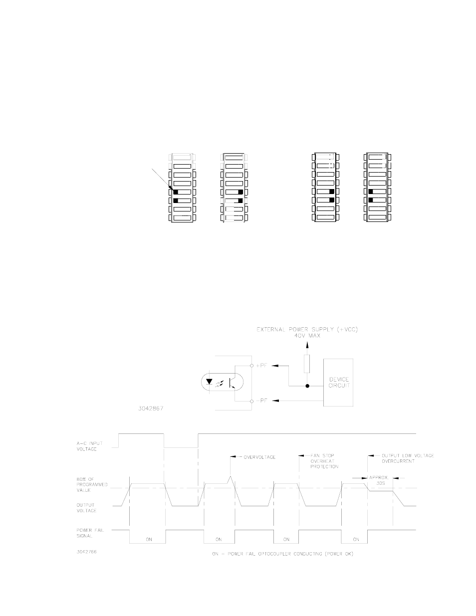
3.8.2.2 OPTICALLY-COUPLED LOGICAL ALARM
The second option uses optically-coupled logic level alarm signals (see PAR. 3.8.2.2), +PF (pin 5
of the rack adapter I/O connector) and -PF (pin 13), provided directly from the Kepco RKE power
supply that is the heart of the HSF power supply. This option is selected by setting positions 5 and
6 of the DIP switches as shown in Figure 9B. Use this option if the power supply will operate
below the minimum voltages specified in Table 4.
FIGURE 9. DIP SWITCH SETTINGS FOR OPTICALLY COUPLED LOGICAL ALARM
The logic alarm circuit is a diode transistor optical coupler (see Figure 10). The transistor is nor-
mally conducting. When the alarm is activated upon detection of power loss, overvoltage, fan
fault, overtemperature or overcurrent condition, the transistor cuts off and the collector emitter cir-
cuit is open. Figure 11 is a timing diagram of the power fail signal.
The default state of the alarm is logic low. The sink current for the optocoupler is 50mA maximum,
the maximum collector to emitter saturation voltage is 0.40 Volts, and the collector to emitter volt-
age is 40 volts maximum. The PF signals are isolated from the AC input and DC output.
FIGURE 10. OUTPUT ALARM CIRCUIT OPTICALLY ISOLATED
FIGURE 11. ±PF POWER FAILURE OPTOCOUPLER TIMING DIAGRAM
3042878
5
5 +PF
+PF 5
5
SW1
-PF 6
6
SW2
6
6 -PF
OFF
ON
OFF
ON
USE N.O. AND N.C CONTACTS
(FACTORY DEFAULT)
OF INTERNAL RELAY
A
LOGICAL ALARM
USE OPTICALLY-COUPLED
B
(+PF AND -PF)
5
6
6
SW1
5
SW2
OFF
ON
ON
OFF
+PF 5
-PF 6
6 -PF
5 +PF
TAB