Burst write, Qphy-ddr2 software option – Teledyne LeCroy QPHY-DDR2 User Manual
Page 9
QPHY-DDR2 Software Option
QPHY-DDR2-OM-E Rev
A
9
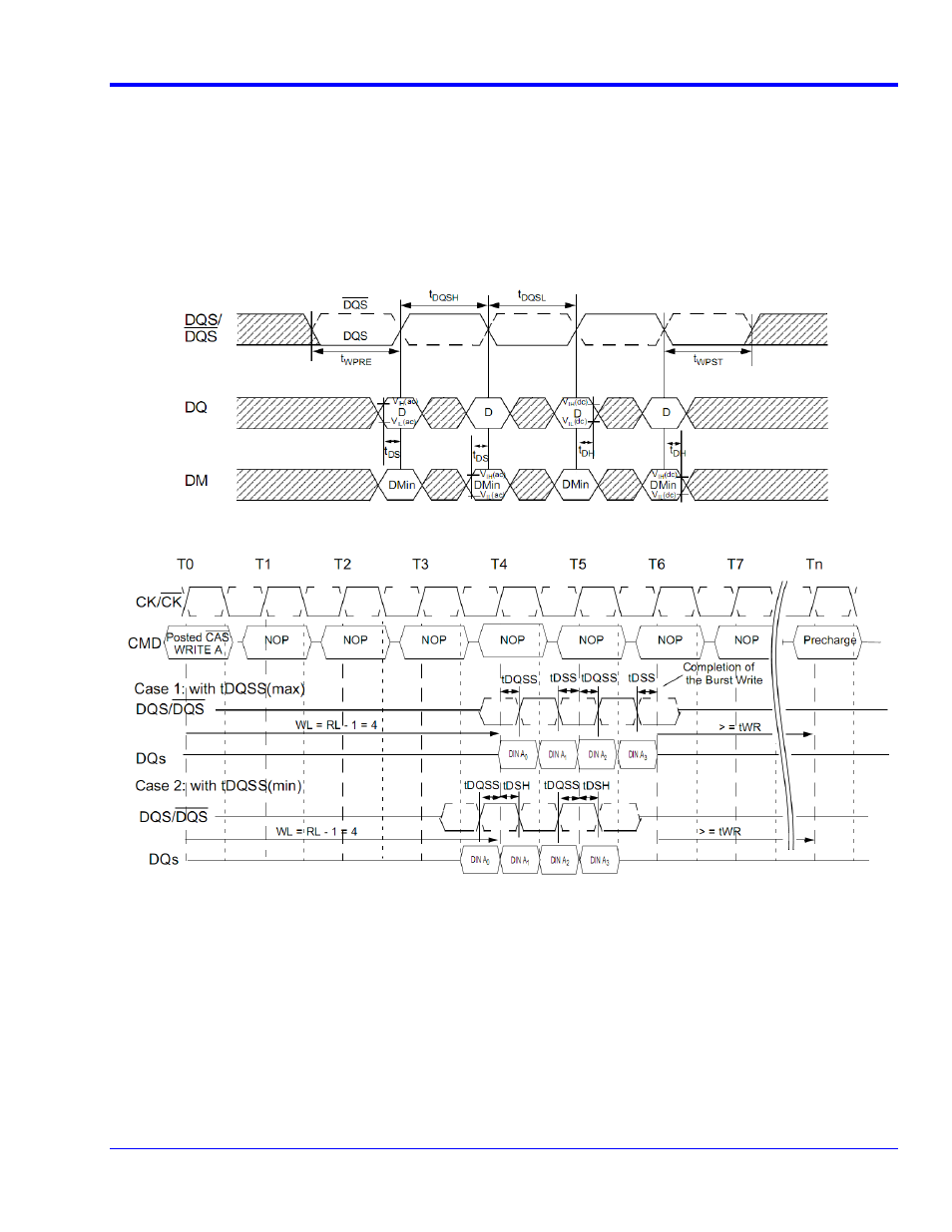
Burst Write
The Burst Write command is initiated by having CS#, CAS# and WE# LOW while holding RAS# HIGH at the rising
edge of the clock. The address inputs determine the starting column address. Write latency (WL) is defined by a
read latency (RL) minus one and is equal to (AL + CL -1); and is the number of clocks of delay that are required
from the time the write command is registered to the clock edge associated to the first DQS strobe. A data strobe
signal (DQS) should be driven LOW (preamble) nominally half clock prior to the [first rising edge]. The first data bit
of the burst cycle must be applied to the DQ pins at the first rising edge of the DQS following the preamble. The
tDQSS specification must be satisfied for each positive DQS transition to its associated clock edge during write
cycles. The subsequent burst bit data are issued on successive edges of the DQS until the burst length is
completed, which is 4 or 8 bit burst.
Figure 3. Data input (write) timing [JESD79-2E figure 38]
Figure 4. Burst write operation [JESD79-2E figure 39]