Burst read – Teledyne LeCroy QPHY-DDR2 User Manual
Page 8
8
QPHY-DDR2-OM-E Rev
A
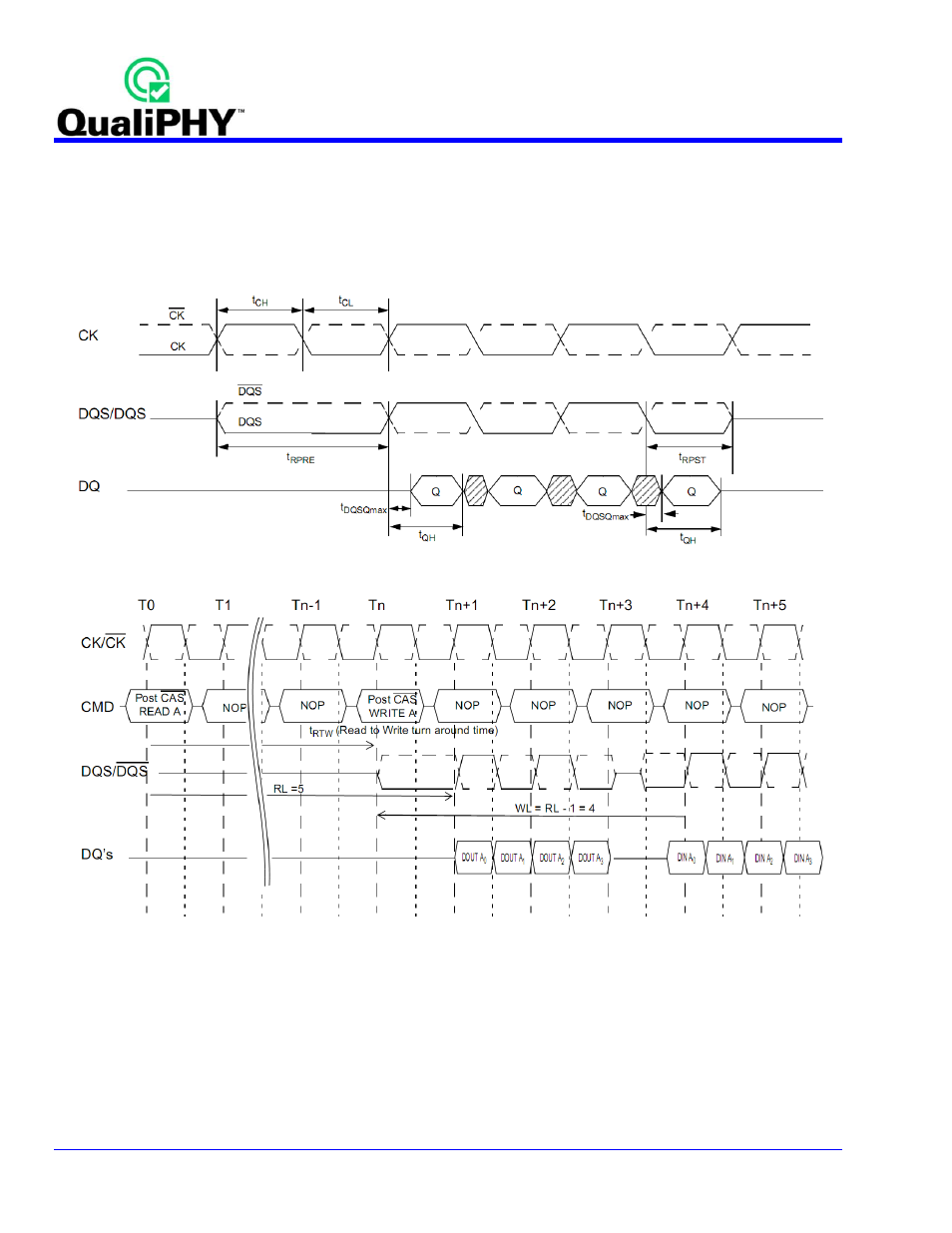
Burst Read
The Burst Read command is initiated by having CS# and CAS# LOW while holding RAS# and WE# HIGH at the
rising edge of the clock. The address inputs determine the starting column address for the burst. The data strobe
output (DQS) is driven LOW one clock cycle before valid data (DQ) is driven onto the data bus. The first bit of the
burst is synchronized with the rising edge of the data strobe (DQS). Each subsequent data-out appears on the DQ
pin in phase with the DQS signal in a source synchronous manner.
Figure 1. Data output (read) timing [JESD79-2E figure 32]
Figure 2. Burst read followed by burst write [JESD79-2E figure 35]
The minimum time from the burst read command to the burst write command is defined by a read-to-write-turn-
around-time, which is 4 clocks in case of BL = 4 operation, 6 clocks in case of BL = 8 operation.
- WaveAce EasyScope Operators Manual (28 pages)
- PeRT3 Software Interface (15 pages)
- FireInspector Automation Application Programming Interface (92 pages)
- PETracer ProtoSync Software User Manual (154 pages)
- QPHY-PCIe3-Tx-Rx (32 pages)
- Signal Integrity Studio (14 pages)
- Serial Data Debug Solutions (204 pages)
- Line Code and Symbolic Decoders (20 pages)
- AORM - Advanced Optical Recording Measurements (125 pages)
- CANbus TD - Quick Reference Guide (8 pages)
- CANbus TD and CANbus TDM - Operators Manual (69 pages)
- FlexRay Trigger, Decode and Physical Layer Test (32 pages)
- MIPI D-PHY (15 pages)
- DFP2 - Digital Filter Package 2 (22 pages)
- ET-PMT - Electrical Telecom Pulse Mask Testing (11 pages)
- ENETbusD Decoder (16 pages)
- Eye Doctor II (45 pages)
- JitKit (16 pages)
- JTA2 (31 pages)
- Power Analyzer Package (34 pages)
- QPHY-10GBase-KR (28 pages)
- QPHY-10GBase-T (36 pages)
- QPHY-BroadR-Reach (33 pages)
- QPHY-DDR3 (44 pages)
- QPHY-DDR4 (73 pages)
- QPHY-DisplayPort (19 pages)
- QPHY-ENET (78 pages)
- QPHY-HDMI (37 pages)
- QPHY-LPDDR2 (49 pages)
- QPHY-MIPI-DPHY (32 pages)
- QPHY-MOST150 (24 pages)
- QPHY-MOST50 (21 pages)
- QPHY-PCIe (30 pages)
- QPHY-PCIE3 (28 pages)
- QPHY-SAS2 (45 pages)
- QPHY-SAS3 (50 pages)
- QPHY-SATA (45 pages)
- QPHY-USB (66 pages)
- QPHY-USB3-Tx-Rx (47 pages)
- QPHY-UWB (30 pages)
- SDA II (38 pages)
- SDA III-CompleteLinQ (59 pages)
- Spectrum Analyzer (14 pages)
- USB2 Decoder (24 pages)