Tih(base) - address and control input hold time, Qphy-ddr2 software option – Teledyne LeCroy QPHY-DDR2 User Manual
Page 47
QPHY-DDR2 Software Option
QPHY-DDR2-OM-E Rev
A
47
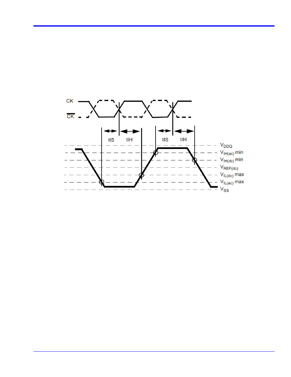
tIH(base) - Address and Control Input Hold Time
Input waveform timing is referenced from the input signal crossing at the VIL(dc)max level to the differential clock
crosspoint at VREF for a rising signal, and from the input signal crossing at the VIH(dc)min level to the differential
clock crosspoint at VREF for a falling signal applied to the device under test. See Figure 31 as follows.
Hold (tIH) nominal slew rate for a rising signal is defined as the slew rate between the last crossing of VIL(dc)max
and the first crossing of VREF(dc). Hold (tIH) nominal slew rate for a falling signal is defined as the slew rate
between the last crossing of VIH(dc)min and the first crossing of VREF(dc).
Jedec JESD79-2E Specific Note 9 (page 95 to 100) with tables 46 and 47 explain the limit compensation versus
the slewrate of the measured signals. Timing limits are initially specified for input slewrate of 1V/ns for single-
ended signals and 2V/ns for differential signal (for DQS and CK).
Figure 31. Differential input waveform timing - tIS and tIH [JESD79-2E figure 99]
§ § §