Tis(base) - address and control input setup time – Teledyne LeCroy QPHY-DDR2 User Manual
Page 46
46
QPHY-DDR2-OM-E Rev
A
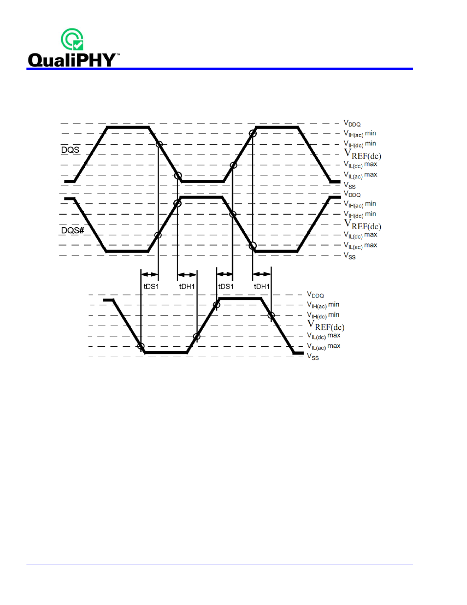
signal must be monotonic between VIL(dc)max and VIH(dc)min. See Figure 30 as follows.
Jedec JESD79-2E Specific Note 8 (page 85 to 94) with table 45 explains the limit compensation versus the
slewrate of the measured signals. Timing limits are initially specified for input slewrate of 1V/ns for single-ended
signals and 2V/ns for differential signal (for DQS and CK).
Figure 30. Single-ended input waveform timing - tDS1 and tDH1
The following tests require probing and address or control signal. These tests are only available in the
configurations using 4 probes.
Prerequisite: SLEW of CK and Address or Control, a derating factor is applied to the limit depending on the
signals slewrate. This is applicable for both of the following tests.
tIS(base) - Address and Control Input Setup Time
Input waveform timing is referenced from the input signal crossing at the VIH(ac)min level to the differential clock
crosspoint at VREF for a rising signal, and from the input signal crossing at the VIL(ac)max level to the differential
clock crosspoint at VREF for a falling signal applied to the device under test. See Figure 31 as follows.
Setup (tIS) nominal slew rate for a rising signal is defined as the slew rate between the last crossing of VREF(dc)
and the first crossing of VIH(ac)min. Setup (tIS) nominal slew rate for a falling signal is defined as the slew rate
between the last crossing of VREF(dc) and the first crossing of VIL(ac)max.
Jedec JESD79-2E Specific Note 9 (page 95 to 100) with tables 46 and 47 explain the limit compensation versus
the slewrate of the measured signals. Timing limits are initially specified for input slewrate of 1V/ns for single-
ended signals and 2V/ns for differential signal (for DQS and CK).